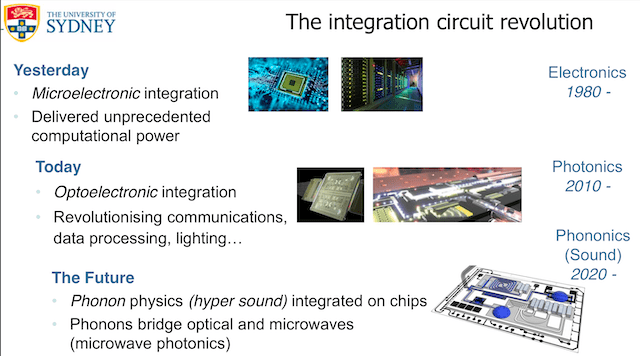
Often science and industry seems to advance from investigating phenomena that is a side effect of something else we want to try to accomplish. Optical fibers have been in use for over a decade now and have always had a problem called Brillouin scattering, where light photon’s interact with surrounding cladding and generate small vibrations or sound packets. This feedback causes light to disperse across the length of the fibre due to Brillouin scattering and create sound packets called phonons aka hyper sound.
As a recent article I read in Science Daily (Wired for sound a third wave emerges in integrated circuits) describes it, the first wave of ICs was based on electronics and was developed after WW II, the second wave was based on photons and came about largely at the start of this century, and now the third wave is emerging based on sound, phonons.
The research team at The University of Sydney, Nano Institute have published over 70 papers on Brillouin scattering and Prof. Benjamin J. Eggleton recently published a summary of their research in a Nature Photonics paper (Brillouin integrated photonics, behind paywall) but one can download the deck he presented as a summary of the paper, at an OSA Optoelectronics Technical Group webinar, last year..

It appears as if the Brillouin scattering technology is particularly useful for (microwave) photonics computing. In the Science Daily article, the professor says that the big advance here is in the control of light and sound over small distances. In the Sarticle, the Professor goes onto say that “Brillouin scattering of light helps us measure material properties, transform how light and sound move through materials, cool down small objects, measure space, time and inertia, and even transport optical information.”
I believe from a photonics IC perspective, transforming how light, other electromagnetic radiation, and sound move through materials is exciting. New technology for measuring material properties, cool down small objects, measure space, time and inertia are also of interest, but not as important in our view.
What’s a phonon
As discussed earlier, phonons are packets of sound vibration above 100mhz, that come about due to optical photons interaction with cladding. As photons bounce off the cladding they generate phonons within the material. Such bouncing creates optical and acoustical waves or phonons.

There’s been a lot of research on how to create “Stimulated Brillouin Scattering” (SBS) on silicon CMOS devices and still goes on, but lately they have found an effective hybrid (Silicon, SiO2, & As2S3) formula to generate SBS at will at chip scale.
What can you do with SBS phonons
Essentially SBS phonons can be used to measure, monitor, alter and increase the flow of electromagnetic (EM) waves in a substance or wave guide. I believe this can be light, microwaves, or just about anything on the EM spectrum. Nothing was mentioned about X-Rays, but it’s just another band of EM radiation.
With SBS, one can supply microwave filters, phase shifters and sources, recover carrier signal in coherent optical communications, store (or delay) light, create lasers and measure, at the sub-mm scale, optical material characteristics. Although the article discusses cooling down materials, I didn’t see anything in the deck describing this.

As SBS technologies are optical-acoustical devices, they are immune to EMI (electro- magnetic interference), EMPs (electro-magnetic pulses) and consume less energy than electronic circuits performing similar functions.
We’ve talked about photonic computing before (see our Photonic computing, seeing the light of day post). But to make photonics a real alternative to electronic computing they need a lot of optical management devices. We discussed a couple in the blog post mentioned above but SBS opens up another dimension of ways to control photonic data flow and processing.
Unclear why the research into SBS seems to be generated out of Australian Universities. However their research is being (at least partially) funded by a number of US DoD entities.

It’s unclear whether SBS will ultimately be one of those innovations in the long run, which enables a new generation of (photonic) IC technologies. But the team has shown that with SBS they can do a lot of useful work with optical/microwave transmission, storage and measurement.
It seems to me that to construct full photonic computing, we need an optical DRAM device. Storing light (with SBS) is a good first step, but any optical store/memory device needs to be randomly accessible, and store Kb, Mb or Gb of optical data, in chip size areas and persist (dynamic refreshing is ok).
The continued use of DRAM for this would make the devices susceptible to EMI, EMP and consume more energy. Maybe something could be done with an all optical 3DX that would suffice as a photonics memory device. Then it could be called Optical DC PM.
So, ICs with electronics, photonics and now phononics are in our future.
Comments?
Photo Credits: