Phonons, the next big technology underpinning integrated circuits

Often science and industry seems to advance from investigating phenomena that is a side effect of something else we want to try to accomplish. Optical fibers have been in use for over a decade now and have always had a problem called Brillouin scattering, where light photon’s interact with surrounding cladding and generate small vibrations or sound packets. This feedback causes light to disperse across the length of the fibre due to Brillouin scattering and create sound packets called phonons aka hyper sound.

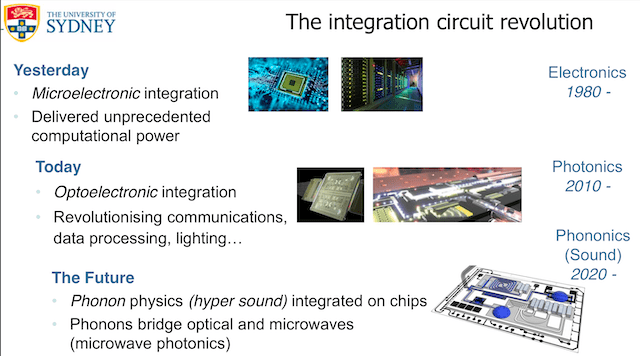
As a recent article I read in Science Daily (Wired for sound a third wave emerges in integrated circuits) describes it, the first wave of ICs was based on electronics and was developed after WW II, the second wave was based on photons and came about largely at the start of this century, and now the third wave is emerging based on sound, phonons.

The research team at The University of Sydney, Nano Institute have published over 70 papers on Brillouin scattering and Prof. Benjamin J. Eggleton recently published a summary of their research in a Nature Photonics paper (Brillouin integrated photonics, behind paywall) but one can download the deck he presented as a summary of the paper, at an OSA Optoelectronics Technical Group webinar, last year..

It appears as if the Brillouin scattering technology is particularly useful for (microwave) photonics computing. In the Science Daily article, the professor says that the big advance here is in the control of light and sound over small distances. In the Sarticle, the Professor goes onto say that “Brillouin scattering of light helps us measure material properties, transform how light and sound move through materials, cool down small objects, measure space, time and inertia, and even transport optical information.”

I believe from a photonics IC perspective, transforming how light, other electromagnetic radiation, and sound move through materials is exciting. New technology for measuring material properties, cool down small objects, measure space, time and inertia are also of interest, but not as important in our view.

What’s a phonon

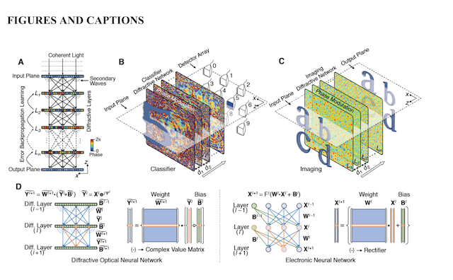
As discussed earlier, phonons are packets of sound vibration above 100mhz, that come about due to optical photons interaction with cladding. As photons bounce off the cladding they generate phonons within the material. Such bouncing creates optical and acoustical waves or phonons.

There’s been a lot of research on how to create “Stimulated Brillouin Scattering” (SBS) on silicon CMOS devices and still goes on, but lately they have found an effective hybrid (Silicon, SiO2, & As2S3) formula to generate SBS at will at chip scale.

What can you do with SBS phonons

Essentially SBS phonons can be used to measure, monitor, alter and increase the flow of electromagnetic (EM) waves in a substance or wave guide. I believe this can be light, microwaves, or just about anything on the EM spectrum. Nothing was mentioned about X-Rays, but it’s just another band of EM radiation.

With SBS, one can supply microwave filters, phase shifters and sources, recover carrier signal in coherent optical communications, store (or delay) light, create lasers and measure, at the sub-mm scale, optical material characteristics. Although the article discusses cooling down materials, I didn’t see anything in the deck describing this.

As SBS technologies are optical-acoustical devices, they are immune to EMI (electro- magnetic interference), EMPs (electro-magnetic pulses) and consume less energy than electronic circuits performing similar functions.

We’ve talked about photonic computing before (see our Photonic computing, seeing the light of day post). But to make photonics a real alternative to electronic computing they need a lot of optical management devices. We discussed a couple in the blog post mentioned above but SBS opens up another dimension of ways to control photonic data flow and processing.

Unclear why the research into SBS seems to be generated out of Australian Universities. However their research is being (at least partially) funded by a number of US DoD entities.

It’s unclear whether SBS will ultimately be one of those innovations in the long run, which enables a new generation of (photonic) IC technologies. But the team has shown that with SBS they can do a lot of useful work with optical/microwave transmission, storage and measurement.

It seems to me that to construct full photonic computing, we need an optical DRAM device. Storing light (with SBS) is a good first step, but any optical store/memory device needs to be randomly accessible, and store Kb, Mb or Gb of optical data, in chip size areas and persist (dynamic refreshing is ok).

The continued use of DRAM for this would make the devices susceptible to EMI, EMP and consume more energy. Maybe something could be done with an all optical 3DX that would suffice as a photonics memory device. Then it could be called Optical DC PM.

So, ICs with electronics, photonics and now phononics are in our future.

Comments?

Photo Credits:

Shedding light on all optical neural networks

Read a couple of articles in the past week or so on all optical neural networks (see All optical neural network (NN) closes performance gap with electronic NN and New design advances optical neural networks that compute at the speed of light using engineered matter).

All optical NN solutions operate faster and use less energy to inference than standard all electronic ones. However, in reality they aree more of a hybrid soulution as they depend on the use of standard ML DL to train a NN. They then use 3D printing and other lithographic processes to create a series diffraction layers of an all optical NN that matches the trained NN.

The latest paper (see: Class-specific Differential Detection in Diffractive Optical Neural Networks Improves Inference Accuracy) describes a significant advance beyond the original solution (see: All-Optical Machine Learning Using Diffractive Deep Neural Networks, Ozcan’s original paper).

How (all optical) Diffractive Deep NNs (DDNNs) work for inferencing

In the original Ozcan discussion, a DDNN consists of a coherent light source (laser), an image, a bunch of refractive and reflective diffraction layers and photo detectors. Each neural network node is represented by a point (pixel?) on a diffractive layer. Node to node connections are represented by lights path moving through the diffractive layer(s).

In Ozcan’s paper, the light flowing through the diffraction layer is modified and passed on to the next diffraction layer. This passing of the light through the diffraction layer is equivalent to the mathematical bias (neural network node FP multiplier) in the trained NN.

The previous challenge has been how to fabricate diffraction layers and took a lot of hand work. But with the advent of 3D printing and other lithographic techniques, nowadays, creating a diffraction layer is relatively easy to do.

In DDNN inferencing, one exposes (via a coherent beam of light) the first diffraction layer to the input image data, then that image is transformed into a different light pattern which is sent down to the next layer. At some point the last diffraction layer converts the light hitting it into classification patterns which is then be detected by photo detectors. Altenatively, the classification pattern can be sent down an all optical computational path (see our Photonic computing sees the light of day post and Photonic FPGAs on the horizon post) to perform some function.

In the original paper, they showed results of an DDNN for a completely connected, 5 layer NN, with 0.2M neurons and 8B connections in total. They also showed results from a sparsely connected, 5 layer NN ,with 0.45M neurons and <0.1B connections

Note, that there’s significant power advantages in exposing an image to a series of diffraction gratings and detecting the classification using a photo detector vs. an all electronic NN which takes an image, uses photo detectors to convert it into an electrical( pixel series) signal and then process it through NN layers performing FP arithmetic at layer node until one reaches the classification layer.

Furthermore, the DDNN operates at the speed of light. The all electronic network seems to operate at FP arithmetic speeds X number of layers. That is only if it could all done in parallel (with GPUs and 1000s of computational engines. If it can’t be done in parallel, one would need to add another factor X the number of nodes in each layer . Let’s just say this is much slower than the speed of light.

Improving DDNN accuracy

The team at UCLA and elsewhere took on the task to improve DDNN accuracy by using more of the optical technology and techniques available to them.

In the new approach they split the image optical data path to create a positive and negative classifier. And use a differential classifier engine as the last step to determine the image’s classification.

It turns out that the new DDNN performed much better than the original DDNN on standard MNIST, Fashion MNIST and another standard AI benchmark.

DDNN inferencing advantages, disadvantages and use cases

Besides the obvious power efficiencies and speed efficiencies of optical DDNN vs. electronic NNs for inferencing, there are a few other advantages:

  • All optical data paths are less noisy – In an electronic inferencing path, each transformation of an image to a pixel file will add some signal loss. In an all optical inferencing engine, this would be eliminated.
  • Smaller inferencing engine – In an electronic inferencing engine one needs CPUs, memory, GPUs, PCIe busses, networking and all the power and cooling to make it work. For an all optical DDNN, one needs a laser, diffraction layers and a set of photo detectors. Yes there’s some electronics involved but not nearly as much as an all electronic NN. And an all electronic NN with 0.5m nodes, and 5 layers with 0.1B connections would take a lot of memory and compute to support. Their DDNN to perform this task took up about 9 cm (3.6″) squared by ~3 to5 cm (1.2″-2.0″) deep.

But there’s some problems with the technology.

  • No re-training or training support – there’s almost no way to re-train the optical DDNN without re-fabricating the DDNN diffraction layers. I suppose additional layers could be added on top of or below the bottom layers, sort of like a corrective lens. Also, if perhaps there was some sort of way to (chemically) develop diffraction layers during training steps then it could provide an all optical DL data flow.
  • No support for non-optical classifications – there’s much more to ML DL NN functionality than optical classification. Perhaps if there were some way to transform non-optical data into optical images then DDNNs could have a broader applicability.

The technology could be very useful in any camera, lidar, sighting scope, telescope image and satellite image classification activities. It could also potentially be used in a heads up displays to identify items of interest in the optical field.

It would also seem easy to adapt DDNN technology to classify analog sensor data as well. It might also lend itself to be used in space, at depth and other extreme environments where an all electronic NN gear might not survive for very long.

Comments?

Photo Credit(s):

Figure 1 from All-Optical Machine Learning Using Diffractive Deep Neural Networks

Figure 2 from All-Optical Machine Learning Using Diffractive Deep Neural Networks

Figure 2 from Class-specific Differential Detection in Diffractive Optical Neural Networks Improves Inference Accuracy

Figure 3 from Class-specific Differential Detection in Diffractive Optical Neural Networks Improves Inference Accuracy

Where should IoT data be processed – part 1

I was at FlashMemorySummit 2019 (FMS2019) this week and there was a lot of talk about computational storage (see our GBoS podcast with Scott Shadley, NGD Systems). There was also a lot of discussion about IoT and the need for data processing done at the edge (or in near-edge computing centers/edge clouds).

At the show, I was talking with Tom Leyden of Excelero and he mentioned there was a real need for some insight on how to determine where IoT data should be processed.

For our discussion let’s assume a multi-layered IoT architecture, with 1000s of sensors at the edge, 100s of near-edge processing/multiplexing stations, and 1 to 3 core data center or cloud regions. Data comes in from the sensors, is sent to near-edge processing/multiplexing and then to the core data center/cloud.

Data size

Dans la nuit des images (Grand Palais) by dalbera (cc) (from flickr)

When deciding where to process data one key aspect is the size of the data. Tin GB or TB but given today’s world, can be PB as well. This lone parameter has multiple impacts and can affect many other considerations, such as the cost and time to transfer the data, cost of data storage, amount of time to process the data, etc. All of these sub-factors include the size of the data to be processed.

Data size can be the largest single determinant of where to process the data. If we are talking about GB of data, it could probably be processed anywhere from the sensor edge, to near-edge station, to core. But if we are talking about TB the processing requirements and time go up substantially and are unlikely to be available at the sensor edge, and may not be available at the near-edge station. And PB take this up to a whole other level and may require processing only at the core due to the infrastructure requirements.

Processing criticality

Human or machine safety may depend on quick processing of sensor data, e. g. in a self-driving car or a factory floor, flood guages, etc.. In these cases, some amount of data (sufficient to insure human/machinge safety) needs to be done at the lowest point in the hierarchy, with the processing power to perform this activity.

This could be in the self-driving car or factory automation that controls a mechanism. Similar situations would probably apply for any robots and auto pilots. Anywhere some IoT sensor array was used to control an entity, that could jeopardize the life of human(s) or the safety of machines would need to do safety level processing at the lowest level in the hierarchy.

If processing doesn’t involve safety, then it could potentially be done at the near-edge stations or at the core. .

Processing time and infrastructure requirements

Although we talked about this in data size above, infrastructure requirements must also play a part in where data is processed. Yes sensors are getting more intelligent and the same goes for near-edge stations. But if you’re processing the data multiple times, say for deep learning, it’s probably better to do this where there’s a bunch of GPUs and some way of keeping the data pipeline running efficiently. The same applies to any data analytics that distributes workloads and data across a gaggle of CPU cores, storage devices, network nodes, etc.

There’s also an efficiency component to this. Computational storage is all about how some workloads can better be accomplished at the storage layer. But the concept applies throughout the hierarchy. Given the infrastructure requirements to process the data, there’s probably one place where it makes the most sense to do this. If it takes a 100 CPU cores to process the data in a timely fashion, it’s probably not going to be done at the sensor level.

Data information funnel

We make the assumption that raw data comes in through sensors, and more processed data is sent to higher layers. This would mean at a minimum, some sort of data compression/compaction would need to be done at each layer below the core.

We were at a conference a while back where they talked about updating deep learning neural networks. It’s possible that each near-edge station could perform a mini-deep learning training cycle and share their learning with the core periodicals, which could then send this information back down to the lowest level to be used, (see our Swarm Intelligence @ #HPEDiscover post).

All this means that there’s a minimal level of processing of the data that needs to go on throughout the hierarchy between access point connections.

Pipe availability

binary data flow

The availability of a networking access point may also have some bearing on where data is processed. For example, a self driving car could generate TB of data a day, but access to a high speed, inexpensive data pipe to send that data may be limited to a service bay and/or a garage connection.

So some processing may need to be done between access point connections. This will need to take place at lower levels. That way, there would be no need to send the data while the car is out on the road but rather it could be sent whenever it’s attached to an access point.

Compliance/archive requirements

Any sensor data probably needs to be stored for a long time and as such will need access to a long term archive. Depending on the extent of this data, it may help dictate where processing is done. That is, if all the raw data needs to be held, then maybe the processing of that data can be deferred until it’s already at the core and on it’s way to archive.

However, any safety oriented data processing needs to be done at the lowest level and may need to be reprocessed higher up in the hierachy. This would be done to insure proper safety decisions were made. And needless the say all this data would need to be held.

~~~~

I started this post with 40 or more factors but that was overkill. In the above, I tried to summarize the 6 critical factors which I would use to determine where IoT data should be processed.

My intent is in a part 2 to this post to work through some examples. If there’s anyone example that you feel may be instructive, please let me know.

Also, if there’s other factors that you would use to determine where to process IoT data let me know.

Smart proteins, the dawn of new intra-cell therapeutics

Saw an article the other day about Smart Cells (Incredible artificial proteins opens up potential for smart cells). There’s another paper that goes into a bit more depth than the original article (‘Limitless potential’ of artificial proteins ushers in new era of ‘smart’ cell therapies).

The two freely available articles talk about two papers in Nature (De novo design of bioactive protein switches & Modular and tunable biological feedback using a de novo protein switch, behind a paywall) that explain the technology in more detail.

Smart proteins act as switches

What the researchers have created is an artificial protein that builds a cage around some bioactive (protein based) mechanism that can be unlocked by another protein while residing in a cell. This new protein is called LOCKR (Latcheable Orthogonal Cage-Key pRotein). LOCKR proteins act as switch activated therapeutics within a cell.

In the picture above the blue coils are the cage proteins and the yellow coil is the bioactive device (protein). Bioactive devices can be designed that degrade other proteins, can modify biological processes within the cell, initiate the cells self-destruct mechanism, etc, just about anything a protein can do within a cell.

In the second Nature paper, they discuss one example of a LOCKR protein, called degron-LOCKR which once inside a cell is used to degrade (destroy) a specific protein. The degron-LOCKR protein only activates when the other protein is active (found) within the cell and it operates only as long as that protein is in sufficient concentration.

The nice thing about the degron-LOCKR protein is that is completely self-regulating. It only operates when the protein to be degraded exists in the cell. That protein acts as the switch in this LOCKR. Until then it remains benign, waiting for a time when the targeted protein starts to be present in the cell.

How LOCKR works

In the picture above the cage is in shown by the grey structure, the bio-active therapy is shown by the yellow structure, and the protein key is shown by the black structure. When the key is introduced into the LOCKR protein, the yellow structure is unfolded (enabled) and can then impact whatever intra-cellular process/protein, it’s been designed to impact.

One key attribute to LOCKR is that the bioactive device within the cage, can be just about anything that works inside the cell. It could be used to create more proteins, less proteins, disable proteins, and perhaps enhance the activity of other proteins.

And, both the LOCKR and the bioactive device can be designed from scratch and fabricated outside or inside the cell. Of course the protein key is the other aspect of the LOCKR mechanism that is fully determined by the designer of the LOCKR protein.

Sort of reminds me of the transistor. Both are essentially switches. For transistors, as long as voltage is applied, it will allow current to flow across the switch. LOCKR does something very similar, but uses a key protein and a bioactive protein that only allows the bioactive protein to activate when the key protein is present.

We’ve talked extensively in the past about using DNA/cells as rudimentary computers and storage, but this takes that technology to a whole other level, (please see our DNA computing series here & here as well as our posts on DNA as storage here & here ). And all that work was done without LOCKR. With LOCKR much of these systems would be even easier to construct and design.

The articles go on to say that LOCKR unleashes the dawn of a new age of intra-cell therapeutics with fine grained control over when and where a particular bio-active therapy is activated within the cell

Some questions

Some of these may be answered in the Nature papers (behind paywall), so sorry in advance, if you have access to those.

How the LOCKR protein(s) are introduced into cells, was not discussed in the freely available articles. We presume that DNA designed to create the LOCKR protein could be injected into cells via a virus, added to the cells DNA via CRISPR, or the LOCKR protein could just be injected into the cell.

Moreover, how LOCKR proteins are scaled up within the cell to be more or less active and scaled up throughout an organ to “fix” multiple cells is yet another question.

Adding artificial DNA or LOCKR proteins to cells may be easy in the lab, but putting such therapy into medical practice will take much time and effort. And any side effects of introducing artificial DNA or LOCKR proteins (not found in nature) to cells will need to be investigated. And finally how such protein technology impacts germ lines would need to be fully understood.

But the fact that the therapeutic process is only active when unlocked by another key protein makes for an intriguing possibility. You would need both the LOCKR protein and the key (unlock-er) protein to be present in a cell for the therapy to be active.

But they present one example, the degron-LOCKR, where the key seems to be a naturally active protein in a cell that needs to be degraded, not a different, artificial protein introduced into the cell. So the key doesn’t have to be an artificial protein and probably would not be for most LOCKR designed proteins.

~~~~

Not a bad start for a new therapy. It has much potential, especially if it can be scaled easily and targeted specifically. Both of which seem doable (given our limited understanding of biological processes).

Comments?

Picture Credit(s): From De novo design of bioactive protein switches article

From Limitless potential… article