New DRAM can be layered on top of CPU cores

At the last IEDM (IEEE International ElectronDevices Meenting), there were two sessions devoted to a new type of DRAM cell that consists or 2 transistors and no capacitors (2TOC) that can be built in layers on top of a micro processor which doesn’t disturb the microprocessor silicon. I couldn’t access (behind paywalls) the actual research but one of the research groups was from Belgium (IMEC) and the other from the US (Notre Dame and R.I.T). This was written up in a couple of teaser articles in the tech press (see IEEE Spectrum tech talk article).

DRAM today is built using 1 transistor and 1 capacitor (1T1C). And it appears that capacitors and logic used for microprocessors aren’t very compatible. As such, most DRAM lives outside the CPU (or microprocessor cores) chip and is attached over a memory bus.

New 2T0C DRAM Bit Cell: Data is written by appliying current to the WBL and WWL and bit’s are read by seeing if acurrent can pass through the RWL RBL

Memory busses have gotten faster in order to allow faster access to DRAM but this to is starting to reach fundamental physical limits and DRAM memory sizes aren’t scaling like the used to.

Wouldn’t it be nice if there were a new type of DRAM that could be easlly built closer or even layered on top of a CPU chip, with faster direct access from/to CPU cores. through inter chip electronics.

Oxide based 2T0C DRAM

DRAM was designed from the start with 1T1C so that it could hold a charge. With a charge in place it could be read out quickly and refreshed periodically without much of a problem.

The researcher found that at certain sizes (and with proper dopants) small transistors can also hold a (small) charge without needing any capacitor.

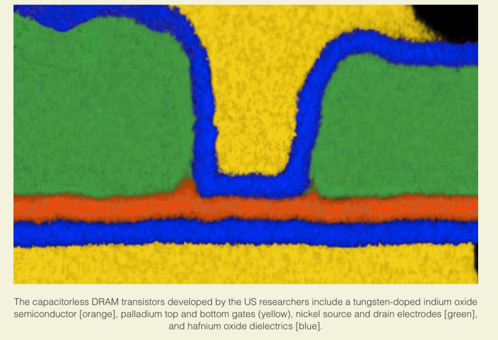
By optimizing the chemistry used to produce those transistors they were able to make 2T0C transistors hold memory values. And given the fabrication ease of these new transistors, they can easily be built on top of CPU cores, at a low enough temperature so as not to disturb the CPU core logic.

But, given these characteristics the new 2T0C DRAMB can also be built up in layers. Just like 3D NAND and unlike current DRAM technologies.

Today 3D NAND is being built at over 64 layers, with Flash NAND roadmap’s showing double or quadruple that number of layers on the horizon. Researchers presenting at IMEC were able to fabricate an 8 layer 2T0C DRAM on top of a microprocessor and provide direct, lightening fast access to it.

The other thing about the new DRAM technology is that it doesn’t need to be refreshed as often. Current DRAM must be refreshed every 64 msec. This new 2T0C technology has a much longer retention time and currently only needs to be refreshed every 400s and much longer retention times are technically feasible.

Some examples of processing needing more memory:

  • AI/ML and the memory wall -Deep learning models are getting so big that memory size is starting to become a limiting factor in AI model effectiveness. And this is just with DRAM today. Optane and other SCM can start to address some of this problem but ithe problem doesn’t go away, AI DL models are just getting more complex I recently read an article where Google trained a trillion parameter language model.
  • In memory databases – SAP HANA is just one example but they are other startups as well as traditional database providers that are starting to use huge amounts of memory to process data at lightening fast speeds. Data only seems to grow not shrink.

Yes Optane and other SCM today can solve some of thise problems. But having a 3D scaleable DRAM memory, that can be built right on chip core, with longer hold times and faster direct access can be a game changer.

It’s unclear whether we will see all DRAM move to the new 2T0C format, but if it can scale well in the Z direction has better access times, and longer retention, it’s unclear why this wouldn’t displace all current 1T1C DRAM over time. However, given the $Bs of R&D spend on new and current DRAM 1T1C fabrication technology, it’s going to be a tough and long battle.

Now if the new 2T0C DRAM could only move from 1 bit per cell to multiple bits per cell, like SLC to MLC NAND, the battle would heat up considerably.

Photo Credits:

New PCM could supply 36PB of memory to CPUs

Read an article this past week on how quantum geometry can enable a new form of PCM (phase change memory) that is based on stacks of metallic layers (SciTech Daily article: Berry curvature memory: quantum geometry enables information storage in metallic layers), That article referred to a Nature article (Berry curvature memory through electrically driven stacking transitions) behind a paywall but I found a pre-print of it, Berry curvature memory through electrically driven stacking transitions.

Figure 1| Signatures of two different electrically-driven phase transitions in WTe2. a, Side view (b–c plane) of unit cell showing possible stacking orders in WTe2 (monoclinic 1T’, polar orthorhombic Td,↑ or Td,↓) and schematics of their Berry curvature distributions in momentum space. The spontaneous polarization and the Berry curvature dipole are labelled as P and D, respectively. The yellow spheres refer to W atoms while the black spheres represent Te atoms. b, Schematic of dual-gate h-BN capped WTe2 evice. c, Electrical conductance G with rectangular-shape hysteresis (labeled as Type I) induced by external doping at 80 K. Pure doping was applied following Vt/dt = Vb/db under a scan sequence indicated by black arrows. d, Electrical conductance G with butterfly-shape switching (labeled as Type II) driven by electric field at 80 K. Pure E field was applied following -Vt/dt = Vb/db under a scan sequence indicated by black arrows. Positive E⊥ is defined along +c axis. Based on the distinct hysteresis observations in c and d, two different phase transitions can be induced by different gating configurations.

The number one challenge in IT today,is that data just keeps growing. 2+ Exabytes today and much more tomorrow.

All that information takes storage, bandwidth and ultimately some form of computation to take advantage of it. While computation, bandwidth, and storage density all keep going up, at some point the energy required to read, write, transmit and compute over all these Exabytes of data will become a significant burden to the world.

PCM and other forms of NVM such as Intel’s Optane PMEM, have brought a step change in how much data can be stored close to server CPUs today. And as, Optane PMEM doesn’t require refresh, it has also reduced the energy required to store and sustain that data over DRAM. I have no doubt that density, energy consumption and performance will continue to improve for these devices over the coming years, if not decades.

In the mean time, researchers are actively pursuing different classes of material that could replace or improve on PCM with even less power, better performance and higher densities. Berry Curvature Memory is the first I’ve seen that has several significant advantages over PCM today.

Berry Curvature Memory (BCM)

I spent some time trying to gain an understanding of Berry Curvatures.. As much as I can gather it’s a quantum-mechanical geometric effect that quantifies the topological characteristics of the entanglement of electrons in a crystal. Suffice it to say, it’s something that can be measured as a elecro-magnetic field that provides phase transitions (on-off) in a metallic crystal at the topological level. 

In the case of BCM, they used three to five atomically thin, mono-layers of  WTe2 (Tungsten Ditelluride), a Type II  Weyl semi-metal that exhibits super conductivity, high magneto-resistance, and the ability to alter interlayer sliding through the use of terahertz (Thz) radiation. 

It appears that by using BCM in a memory, 

Fig. 4| Layer-parity selective Berry curvature memory behavior in Td,↑ to Td,↓ stacking transition. a,
The nonlinear Hall effect measurement schematics. An applied current flow along the a axis results in the generation of nonlinear Hall voltage along the b axis, proportional to the Berry curvature dipole strength at the Fermi level. b, Quadratic amplitude of nonlinear transverse voltage at 2ω as a function of longitudinal current at ω. c, d, Electric field dependent longitudinal conductance (upper figure) and nonlinear Hall signal (lower figure) in trilayer WTe2 and four-layer WTe2 respectively. Though similar butterfly-shape hysteresis in longitudinal conductance are observed, the sign of the nonlinear Hall signal was observed to be reversed in the trilayer while maintaining unchanged in the four-layer crystal. Because the nonlinear Hall signal (V⊥,2ω / (V//,ω)2 ) is proportional to Berry curvature dipole strength, it indicates the flipping of Berry curvature dipole only occurs in trilayer. e, Schematics of layer-parity selective symmetry operations effectively transforming Td,↑ to Td,↓. The interlayer sliding transition between these two ferroelectric stackings is equivalent to an inversion operation in odd layer while a mirror operation respect to the ab plane in even layer. f, g, Calculated Berry curvature Ωc distribution in 2D Brillouin zone at the Fermi level for Td,↑ and Td,↓ in trilayer and four-layer WTe2. The symmetry operation analysis and first principle calculations confirm Berry curvature and its dipole sign reversal in trilayer while invariant in four-layer, leading to the observed layer-parity selective nonlinear Hall memory behavior.
  • To alter a memory cell takes “a few meV/unit cell, two orders of magnitude less than conventional bond rearrangement in phase change materials” (PCM). Which in laymen’s terms says it takes 100X less energy to change a bit than PCM.
  • To alter a memory cell it uses terahertz radiation (Thz) this uses pulses of light or other electromagnetic radiation whose wavelength is on the order of picoseconds or less to change a memory cell. This is 1000X faster than other PCM that exist today.
  • To construct a BCM memory cell takes between 13 and 16  atoms of W and Te2 constructed of 3 to 5 layers of atomically thin, WTe2 semi-metal.

While it’s hard to see in the figure above, the way this memory works is that the inner layer slides left to right with respect to the picture and it’s this realignment of atoms between the three or five layers that give rise to the changes in the Berry Curvature phase space or provide on-off switching.

To get from the lab to product is a long road but the fact that it has density, energy and speed advantages measured in multiple orders of magnitude certainly bode well for it’s potential to disrupt current PCM technologies.

Potential problems with BCM

Nonetheless, even though it exhibits superior performance characteritics with respect to PCM, there are a number of possible issues that could limit it’s use.

One concern (on my part) is that the inner-layer sliding may induce some sort of fatigue. Although, I’ve heard that mechanical fatigue at the atomic level is not nearly as much of a concern as one sees in (> atomic scale and) larger structures. I must assume this would induce some stress and as such, limit the (Write cycles) endurance of BCM.

Another possible concern is how to shrink size of the Thz radiation required to only write a small area of the material. Yes one memory cell can be measured bi the width of 3 atoms, but the next question is how far away do I need to place the next memory cell. The laser used in BCM focused down to ~1.5 μm. At this size it’s 1,000X bigger than the BCM memory cell width (~1.5 nm).

Yet another potential problem is that current BCM must be embedded in a continuous flow of liquid nitrogen (@80K). Unclear how much of a requirement this temperature is for BCM to function. But there are no computers nowadays that require this level of cooling.

Figure 3| Td,↑ to Td,↓ stacking transitions with preserved crystal orientation in Type II hysteresis. a,
in-situ SHG intensity evolution in Type II phase transition, driven by a pure E field sweep on a four-layer and a five-layer Td-WTe2 devices (indicated by the arrows). Both show butterfly-shape SHG intensity hysteresis responses as a signature of ferroelectric switching between upward and downward polarization phases. The intensity minima at turning points in four-layer and five-layer crystals show significant difference in magnitude, consistent with the layer dependent SHG contrast in 1T’ stacking. This suggests changes in stacking structures take place during the Type II phase transition, which may involve 1T’ stacking as the intermediate state. b, Raman spectra of both interlayer and intralayer vibrations of fully poled upward and downward polarization phases in the 5L sample, showing nearly identical characteristic phonons of polar Td crystals. c, SHG intensity of fully poled upward and downward polarization phases as a function of analyzer polarization angle, with fixed incident polarization along p direction (or b axis). Both the polarization patterns and lobe orientations of these two phases are almost the same and can be well fitted based on the second order susceptibility matrix of Pm space group (Supplementary Information Section I). These observations reveal the transition between Td,↑ and Td,↓ stacking orders is the origin of
Type II phase transition, through which the crystal orientations are preserved.

Finally, from my perspective, can such a memory can be stacked vertically, with a higher number of layers. Yes there are three to five layers of the WTe2 used in BCM but can you put another three to five layers on top of that, and then another. Although the researchers used three, four and five layer configurations, it appears that although it changed the amplitude of the Berry Curvature effect, it didn’t seem to add more states to the transition.. If we were to more layers of WTe2 would we be able to discern say 16 different states (like QLC NAND today).

~~~~

So there’s a ways to go to productize BCM. But, aside from eliminating the low-temperature requirements, everything else looks pretty doable, at least to me.

I think it would open up a whole new dimension of applications, if we had say 60TB of memory to compute with, don’t you think?

Comments?

[Updated the title from 60TB to PB to 36PB as I understood how much memory PMEM can provide today…, the Eds.]

Photo Credit(s):

Need memory, Intel’s Optane DC PM to the rescue

I attended Intel’s DataCentric Innovation Conference Tech Field Day eXclusive (TFDx) last April. There were a couple of items Intel presented at the show that peaked my interest there, one of which was DL Boost (see my Intel’s new DL Boost for AI inferencing blog post) and the other was Optane DC PM (data center persistent memory). This post is about Optane DC PM.

As you already know, Optane SSDs have been on the market now for at least a year or so and have not gained much market traction as of yet. I and others attribute this to the high price differential between Optane SSDs and NVMe Flash SSDs but others may say it’s a matter of production yields – probably a little of both.

But Optane, as announced, always had another form factor (if that’s the right term), as persistent memory that could dramatically increase the size of server memory to support new memory intensive applications at a lower price than DRAM.

I was at Nutanix .NEXT conference last week and saw a 4 socket server from DELL that had 6TB of DRAM in it (and 4-44 core CPUs). I didn’t ask the price but when I mentioned I wanted one for my home office, they said it could easily heat my house. So the other problem with a lot of DRAM is power consumption.

Optane DC PM (data center persistent) memory is intended to solve both the high cost and high power consumption problems of DRAM.

How does it work in a server

The newer Intel motherboards support up to 12 slots of memory per socket. And up to 6 of these can be Optane DC PM (512GB DIMM) or 3TB per socket. Optane DC PM is accessed via L1-L2 caching just like any other memory. Apparently with a dual socket system you can have up to 11 Optane DC PM DIMMs on the motherboard.

L1-L2 cache access times are on the order of picoseconds (10**[-12] seconds), DRAM is on the order of nanoseconds (10**[-9] seconds) and flash is on the order of 100 microseconds (100*10**[-6] seconds). So there’s a vast access time gulf between DRAM and Flash that could be exploited with the right technology – enter Optane DC PM.

The only detailed info I could find on Optane DC PM access times was in a research paper (see Basic performance of Intel Optane DC PMM research paper) and it said Optane DC PM assessing times are ~350 nanoseconds, or close to right between DRAM and Flash. At the show the development team indicated that Optane DC PM support about 3GB/sec of bandwidth per module (DIMM).

There are two ways to use Optane DC PM:

  1. Memory mode – in Memory mode, the data in Optane DC PM is thrown away during a power cycle. You must use a block of DRAM as a cache or rather a virtual memory block to the Optane DC PM acting as a paging store. Data is brought into the DRAM cache when accessed using its (virtual) DRAM address and when no longer used. it gets evicted (destaged) back out to Optane DC PM. When power is cycled the data in Optane DC PM is cleared out. Optane DC PM supports AES XTS-256 bit encryption and can easily be cleared by throwing away encryption keys during a power cycle.
  2. App Direct mode – in App Direct mode, Optane DC PM is accessed directly using application APIs and its data persists across power cycles. For App Direct mode, Optane DC PM is still AES 256 encrypted but here the encryption key is maintained across power cycles but is locked on power up and you need to use a pass phrase to unlock it. In this mode, applications are responsible for flushing (L1-L2) caches to Optane to retains all data written through L1-L2 to the Optane DC PM. There’s a GitHub Persistent Memory Development Kit (PMDK) library for that supports the App Direct mode API that applications need to use.

Both modes use DDR-T, (transactional DDR4) a new memory bus protocol for Optane DC PM access. In the DDR-T protocol, access to the memory bus is requested by a CPU and is granted by an Optane DC PM DIMM. All Optane DC PM DIMMs on a system can be accessed in parrallel.

You can use RDMA to replicate (App direct?) Optane DC PM data from one system to another. In order to support Memory and App Direct mode, Optane DC PM required CPU, BIOS and (application) software changes.

Most of the Optane DC PM support and cryptology logic is implemented in hardware. Optane DC PM has an address indirection table (AIT) to support 3D XPoint wear leveling maintained in DRAM but flushed to Optane during power loss. Transfers to 3D XPoint media is in 256 byte cache lines but the memory bus operates in 64 byte cache lines, so there’s a (DRAM) buffer between media and memory bus.

Optane also supports a high availability, or up to two device failure mode. In this scenario, if one Optane DC PM DIMM fails, the system can swap another spare Optane DC PM DIMM into that address space and continue to operate. If a 2nd Optane DC PM fails then the system fails. Not sure what happens to the data on the original Optane DC PM DIMM during a failure. It seems to me data would be lost, but it could depend on its failure mode.

In Memory mode, the expected ratio between DRAM size and Optane DC PM size is should be 32GB DRAM/6TB Optane DC PM. At the TFDx event, the Optane DC PM team had some performance charts showing different DRAM cache miss rates. Intel also announced new CPU monitoring statistics to track application/workloads impacting DRAM/Optane DC PM in Memory mode and to track Optane DC PM health.

Optane DC PM usage modes are established by the BIOS. It’s flexible enough to have the Optane DC PM usage modes be defined on a region by region basis. Not exactly sure what a region is, but it could be an address range spanning MB(?) of Optane DC PM. With both modes in operation on a system, data can be moved from Memory mode Optane to App direct mode Optane or vice versa.

Intel expects that lifetime of an Optane DC PM DIMM to be from 200-370PB of data writes. Optane DC PMs have a 5 year warrantee. Given its bandwidth (3GB/sec), 200PB of data writes should last ~2 years but that’s at 100% duty cycle, writing 3GB of data, every second of every day. So, 5 years should be a reasonable guarantee using a more realistic ~40% duty cycle.

What applications use Optane DC PM

The one of interest to most people seems to be SAP HANA. According to the development team, SAP HANA could use App Direct mode for main database storage and use DRAM for its delta column store. Cassandra could also use Optane in App Direct mode in a similar fashion.

Also something like a REDIS for key-value store could use Optane DC PM to store Values and use DRAM to store Keys.

But any application could take advantage of the extra memory made available with Optane DC PM DIMMs in Memory mode today. Of course any use of Optane DC PM would require the right levels of Intel Xeon CPUs (Cascade Lake), BIOSes and motherboards.

~~~~

Interested in learning more, TFDx videos of the event are available on the website noted previously. Also these TFDx bloggers also have posts specifically on Optane DC PM.

The coolest thing since sliced bread – Optane by Matt Leib, (@MBLeib)

Intel’s crossover point: A 3D spork by Stephen Foskett (@SFoskett)

Intel answering SAP HANA’s tough questions by Keith Townsend (@CTOAdvisor)

Comments?

New chip architecture with CPU, storage & sensors in one package

Read an article the other day in MIT news, (3D chip combines computing and data storage) about a new 3D chip out of Stanford and MIT research, which includes CPU, RRAM (resistive RAM) storage class memories and sensors in one single package. Such a chip architecture vastly minimizes the off chip bottleneck to access storage and sensors.

Chip componentry

The chip’s sensors are based on carbon nanotubes. Aside from a layer of silicon at the bottom, all the rest of transistors used in the chip are also based off of carbon nanotube FET (field effect transistors).

The RRAM storage class memory is a based on a dielectric material which uses electrical resistance to store non-volatile data.

The bottom layer is a silicon based CPU. On top of the silicon is a carbon nanotube layer. Next comes the RRAM and the top layer is more carbon nanotubes making up the sensor array.

Architectural benefits

One obvious benefit is having data storage directly accessible to the CPU is that there’s no longer a need to go off chip to access data. The 2nd major advantage to the chip architecture is that the sensor array can write directly to RRAM storage, so there’s no off chip delay to provide sensor readout and storage.

Another advantage to using carbon nanotube FET’s is that they can be an order of magnitude more energy efficient than silicon transistors. Moreover, RRAM has the potential to be much denser than DRAM.

Finally, another major advantage is that this can all be built in one 3D chip because carbon nanotube and RRAM fabrication can be done at relatively cooler temperatures (~200C) vs. silicon fabrication which requires relatively high temperatures (1000C). Silicon cannot be readily fabricated in multiple layers because of the high temperatures required which will harm lower layers. But you could fabricate the lowest layer in silicon and then the rest as either carbon nanotube FETs or RRAM without harming the silicon layer.

Transistor/RRAM counts

The chip as fabricated has a million RRAM cells (bits?) and 2 million nanotube FETs. In contrast, in 2014, Intel’s 15-core Xeon Ivy Bridge EX had 4.3B transistors and current DRAM chips offer 64Gb. So there’s a ways to go before carbon nanotube and RRAM densities can get to a level available from silicon today.

However, as they have a bottom layer of silicon they can have all the CPU complexity of an Intel processor and still build RRAM and carbon nanotubes FETs on top of that. Which makes this chip architecture compatible with current CMOS fabrication techniques and a very interesting addition to current CPU architectures.

~~~~

Unclear to me why they stopped at 4 layers (1-silicon FET, 1 carbon nanotubes FET, 1 RRAM and 1 carbon nanotubes FET [sensor array]). If they can do 4 why not do 5 or more. That way they could pack in even more RRAM storage and perhaps more sensor layers.

Also, not sure what the bottom most layer of carbon nanotubes is doing. If I had to hazard a guess, it’s being used for RRAM control logic. But I could be wrong.

I could see how these chips could be used for very specialized sensor applications, with a limited need for data storage. The researchers claim many types of sensors can be created using carbon nanotubes. If that’s the case, maybe we might see these sorts of chips showing up all over the place.

Comments?

Photo Credit(s): Three dimensional integration of nanotechnologies for computing and data storage on a single chip, Nature magazine.