At the last IEDM (IEEE International ElectronDevices Meenting), there were two sessions devoted to a new type of DRAM cell that consists or 2 transistors and no capacitors (2TOC) that can be built in layers on top of a micro processor which doesn’t disturb the microprocessor silicon. I couldn’t access (behind paywalls) the actual research but one of the research groups was from Belgium (IMEC) and the other from the US (Notre Dame and R.I.T). This was written up in a couple of teaser articles in the tech press (see IEEE Spectrum tech talk article).
DRAM today is built using 1 transistor and 1 capacitor (1T1C). And it appears that capacitors and logic used for microprocessors aren’t very compatible. As such, most DRAM lives outside the CPU (or microprocessor cores) chip and is attached over a memory bus.
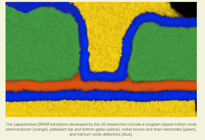
New 2T0C DRAM Bit Cell: Data is written by appliying current to the WBL and WWL and bit’s are read by seeing if acurrent can pass through the RWL RBL
Memory busses have gotten faster in order to allow faster access to DRAM but this to is starting to reach fundamental physical limits and DRAM memory sizes aren’t scaling like the used to.
Wouldn’t it be nice if there were a new type of DRAM that could be easlly built closer or even layered on top of a CPU chip, with faster direct access from/to CPU cores. through inter chip electronics.
Oxide based 2T0C DRAM
DRAM was designed from the start with 1T1C so that it could hold a charge. With a charge in place it could be read out quickly and refreshed periodically without much of a problem.
The researcher found that at certain sizes (and with proper dopants) small transistors can also hold a (small) charge without needing any capacitor.
By optimizing the chemistry used to produce those transistors they were able to make 2T0C transistors hold memory values. And given the fabrication ease of these new transistors, they can easily be built on top of CPU cores, at a low enough temperature so as not to disturb the CPU core logic.
But, given these characteristics the new 2T0C DRAMB can also be built up in layers. Just like 3D NAND and unlike current DRAM technologies.
Today 3D NAND is being built at over 64 layers, with Flash NAND roadmap’s showing double or quadruple that number of layers on the horizon. Researchers presenting at IMEC were able to fabricate an 8 layer 2T0C DRAM on top of a microprocessor and provide direct, lightening fast access to it.
The other thing about the new DRAM technology is that it doesn’t need to be refreshed as often. Current DRAM must be refreshed every 64 msec. This new 2T0C technology has a much longer retention time and currently only needs to be refreshed every 400s and much longer retention times are technically feasible.
Some examples of processing needing more memory:
AI/ML and the memory wall -Deep learning models are getting so big that memory size is starting to become a limiting factor in AI model effectiveness. And this is just with DRAM today. Optane and other SCM can start to address some of this problem but ithe problem doesn’t go away, AI DL models are just getting more complex I recently read an article where Google trained a trillion parameter language model.
In memory databases – SAP HANA is just one example but they are other startups as well as traditional database providers that are starting to use huge amounts of memory to process data at lightening fast speeds. Data only seems to grow not shrink.
Yes Optane and other SCM today can solve some of thise problems. But having a 3D scaleable DRAM memory, that can be built right on chip core, with longer hold times and faster direct access can be a game changer.
It’s unclear whether we will see all DRAM move to the new 2T0C format, but if it can scale well in the Z direction has better access times, and longer retention, it’s unclear why this wouldn’t displace all current 1T1C DRAM over time. However, given the $Bs of R&D spend on new and current DRAM 1T1C fabrication technology, it’s going to be a tough and long battle.
Now if the new 2T0C DRAM could only move from 1 bit per cell to multiple bits per cell, like SLC to MLC NAND, the battle would heat up considerably.
MinIO presented at SFD21 a couple of weeks back (see videos here). They had a great session, as always with Jonathan and AB leading the charge. We’ve had a couple of GreyBeardsOnStorage podcasts with AB as well (listen and see GreyBeards talk open source S3… and GreyBeards talk Data Persistence …). We first talked with MinIO last year at SFD 19 where AB made a great impression on the bloggers (see videos here)
Their customers run the gamut from startups to F500. AB said that ~58% of the F500 have MinIO installed and over 8% of the F500 have added capacity over the last year. AB said they have a big presence in Finance, e.g., the 10 largest banks run MinIO, also the auto and Space/Defense sectors have adopted their product.
One reason for the later two sectors (auto & space/defense) is the size of MinIO’s binary, 50MB. And my guess for why the rest of those customers have adopted MinIO is because it’s S3 API compatible, it’s open source, and it’s relatively inexpensive.
Object storage trends
Customers running in the cloud have a love-hate relationship with object storage, they love that it scales but hate what it costs. There are numerous on prem object storage alternatives from traditional and non-traditional storage vendors, but most are deployed on appliances.
With appliances, customers have to order, wait for delivery, rack-configure-set up and after maybe weeks to months finally they have object storage on prem. But with MinIO a purely software, open source solution, it can be tried by merely downloading a couple of (Docker) containers and deployed/activated in under an hour..
As mentioned above, MinIO is API compatible with AWS S3 which helps with adoption. Moreover, now that it’s an integral part of VMware (see their new Data Persistence Platform), it can be enabled in seconds on your standard enterprise VMware cluster with Tanzu.
The other trend is that the edge needs storage, and lots of it. The main drivers of massive edge storage requirement are TelCos deploying 5G and auto industry’s self-driving cars. But this is just a start, industrial IoT will be generating reams of sensor log data at the edge, it will need to be stored somewhere. And what better place to store all this data, but on object storage. Furthermore, all this is driving more adoption of object storage, with MinIO picking up the lion’s share of deployments.
In addition, MinIO recently ported their software to run on ARM. AB said this was to support the expanding hobbyist and developers community driving edge innovation.
And then there was Kubernetes. Everyone in the industry (with the possible exception of Google) is surprised by the adoption of K8S. Google essentially gifted ~$1Bs in R&D on how to scale apps to the world of IT, and now any startup, anywhere, can scale with as well as Google can. And scaling is the “killer app” for the SW industry.
But performance isn’t bad either
Jonathan made mention of MinIO performance (see MinIO 24 node disk and MinIo 32 node NVMe SSD reports) benchmarks. Their disk data shows avg read and write performance of 16.3GB/s and 9.4GB/s, respectively and their NVMe SSD average read and write performance of 183.2GB/s and 171.3GB/s, respectively. The disk numbers are very good for object storage, but the SSD numbers are spectacular.
It turns out that modern, cloud native apps don’t need quick access to data as much as high data throughput. Modern apps have moved to a processing data in memory rather than off of storage, which means they move (large) chunks of data to memory and crunch on it there, and then spit it back out to storage This type of operating mode seems to scale better (in the cloud at least) than having a high priced storage system servicing a blizzard of IO requests from everywhere.
Other vendors had offered SSD object storage before but it never took off. But nowadays, with NVMe SSDs, MinIO is seeing starting to see healthcare, finance, and any AI/ML workloads all deploying NVMe SSD object storage. Yes for large storage repositories, (object storage’s traditional strongpoint), ie, 5PB to 100PB, disk can’t be beat but where blistering high throughput, is needed, NVMe SSD object storage is the way to go.
Open source vs. open core
AB mentioned that MinIO business model is 100% open source vs. many other vendors that use open source but whose business model is open core. The distinction is that open core vendors use open source as base functionality and then build proprietary, charged for, software features/functions on top of this.
But open source vendors, like MinIO offer all their functionality under an open source license (Apache SM License V2.0, GNU AGPL v3 Open Source license and other FOSS licenses), but if you want to use it commercially, build products with it embedded inside, or have enterprise class support, one purchases a commercial license.
As presented at SFD21, but their website home page has updated numbers reflected below
The pure open source model has some natural advantages:
It’s a great lead gen solution because anyone, worldwide, 7X24X365 can download the software and start using it, (see Docker Hub or MinIO’s download page
It’s a great hiring pool. Anyone, who has contributed to the MinIO open source is potentially a great technical hire. MinIO stats says they have 685 contributors, 19 in just the last month for MinIO base code (see MinIO’s GitHub repo).
It’s a great development organization. With ~20 commits a weekover the last year, there’s a lot going on to add functionality/fix bugs. But that’s the new world of software development. Given all this activity, release frequencies increase, ~4 releases a month ((see GitHub repo insights above).
It’s a great testing pool with, ~480M Docker Pulls (using a Docker container to run a standard, already configured MinIO server, mc, console, etc.) and ~18K enterprises running their solution, that’s an awful lot of users. With open source a lot of eye’s or contributors make all problems visible, but what’s more typical, from my perspective, is the more users that deploy your product, the more bugs they find.
Indeed, with the VMware’s Data Persistence Platform, Tanzu customers can use MinIO’s object storage at the click of a button (or three).
Of course, open source has downsides too. Anyone can access packages directly (from GitHub repo and elsewhere) and use your software. And of course, they can clone, fork and modify your source code, to add any functionality they want to it. Historically, open source subscription licensing models don’t generate as much revenues as appliance purchases do. And finally, open source, because it’s created by geeks, is typically difficult to deploy, configure, and use.
But can they meet the requirements of an Enterprise world
Because most open source is difficult to use, the enterprise has generally shied away from it. But that’s where there’s been a lot of changes to MinIO.
MinIO always had a “mc” (minio [admin] client) that offered a number of administrative services via an API, programmatically controlled interface. but they have recently come out with a GUI offering, the minIO console, which has a similarly functionality to their mc APU. They demoed the console on their SFD21 sessions (see videos above).
Supporting 18K enterprise users, even if only 8% are using it a lot, can be a challenge, but supporting almost a half a billion docker pulls (even if only 1/4th of these is a complete minIO deployment) can be hell on earth. The surprising thing is that MinIO’s commercial license promises customers direct-to-engineer support.
At their SFD21 sessions, AB stated they were getting ~2.7 new (tickets) problems a day. I assume these are what’s just coming in from commercial licensed users and not the general public (using their open source licensed offerings). AB said their average resolution time for these tickets was under 15 minutes.
Enter SubNet, the MinIO Subscription Network and their secret (not open source?) weapon to scale enterprise class support. Their direct-to-engineer support model involves a much, more collaborative approach to solving customer problems then you typical enterprise support with level 1, 2 & 3 support engineers. They demoed SubNet briefly at SFD21, but it could deserve a much longer discussion/demostration.
What little we saw (at SFD21) was that it looked almost like slack-PM dialog between customer and engineer but with unlimited downloads and realtime interaction.
MinIO also supports a very active Slack discussion group with ~11K users. Here anyone can ask a question and it will get answered by anyone. MinIO’s Slack has 2 channels: (Ggeneral and GitHub for notifications). It seems like MinIO is using Slack as a crowdsourced level 1 support.
But in the long run, to continue to offer “direct-to-engineer” levels of support, may require adding a whole lot more engineers. But AB seems prepared to do just that.
~~~~
MinIO is an interesting open source S3 API compatible, object storage solution that seems to run just about anywhere, is freely deployable with enterprise class support available (at a price) and has high throughput performance. What’s not to like.
There’s something happening to the IT industry, that maybe has not happened in a couple of decades or so but hardware innovation is back. We’ve been covering bits and pieces of it in our hardware vs software innovation series (see Open source ASiCs – HW vs. SW innovation [round 5] post).
But first please take our new poll:
Hardware innovation never really went away, Intel, AMD, Apple and others had always worked on new compute chips. DRAM and NAND also have taken giant leaps over the last two decades. These were all major hardware suppliers. But special purpose chips, non CPU compute engines, and hardware accelerators had been relegated to the dustbins of history as the CPU giants kept assimilating their functionality into the next round of CPU chips.
But for some reason it didn’t stop there. We first started seeing some inklings of new hardware innovation in the AI space with a number of special purpose DL NN accelerators coming online over the last 5 years or so (see Google TPU, SC20-Cerebras, GraphCore GC2 IPU chip, AI at the Edge Mythic and Syntiants IPU chips, and neuromorphic chips from BrainChip, Intel, IBM , others). Again, one could look at these as taking the SIMD model of GPUs into a slightly different direction. It’s probably one reason that GPUs were so useful for AI-ML-DL but further accelerations were now possible.
But it hasn’t stopped there either. In the last year or so we have seen SPUs (Nebulon Storage), DPUs (Fungible,NVIDIA Networking, others), and computational storage (NGD Systems, ScaleFlux Storage, others) all come online and become available to the enterprise. And most of these are for more normal workload environments, i.e., not AI-ML-DL workloads,
I thought at first these were just FPGAs implementing different logic but now I understand that many of these include ASICs as well. Most of these incorporate a standard von Neumann CPU (mostly ARM) along with special purpose hardware to speed up certain types of processing (such as low latency data transfer, encryption, compression, etc.).
What happened?
It’s pretty easy to understand why non-von Neumann computing architectures should come about. Witness all those new AI-ML-DL chips that have become available. And why these would be implemented outside the normal X86-ARM CPU environment.
But SPU, DPUs and computational storage, all have typical von Neumann CPUs (mostly ARM) as well as other special purpose logic on them.
Why?
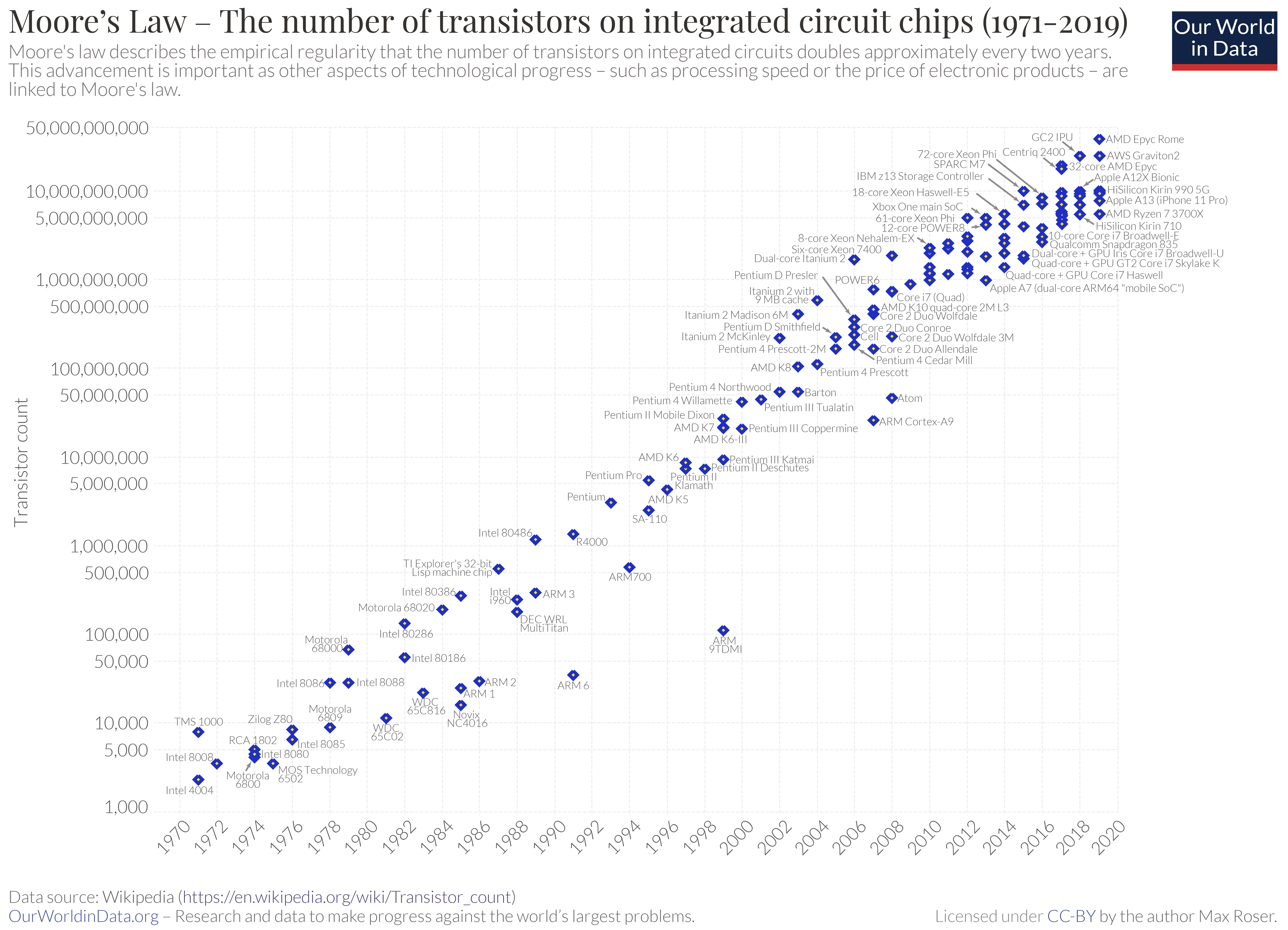
I believe there are a few reasons, but the main two are that Moore’s law (every 2 years halving the size of transistors, effectively doubling transistor counts in same area) is slowing down and Dennard scaling (as you reduce the size of transistors their power consumption goes down and speed goes up) has stopped almost. Both of these have caused major CPU chip manufacturers to focus on adding cores to boost performance rather than just adding more transistors to the same core to increase functionality.
This hasn’t stopped adding instruction functionality to each CPU, but it has slowed considerably. And single (core) processor speeds (GHz) have reached a plateau.
But what it has stopped is having the real estate available on a CPU chip to absorb lots of additional hardware functionality. Which had been the case since the 1980’s.
Hardware design is getting easier & chip fabrication is becoming a commodity
We wrote a post a couple of weeks back talking about an open foundry (see HW vs. SW innovation round 5 noted above)that would take a hardware design and manufacture the ASICs for you for free (or at little cost). This says that the tool chain to perform chip design is becoming more standardized and much less complex. Does this mean that it takes less than 18 months to create an ASIC. I don’t know but it seems so.
But the real interesting aspect of this is that world class foundries are now available outside the major CPU developers. And these foundries, for a fair but high price, would be glad to fabricate a 1000 or million chips for you.
Yes your basic state of the art fab probably costs $12B plus these days. But all that has meant is that A) they will take any chip design and manufacture it, B) they need to keep the factory volume up by manufacturing chips in order to amortize the FAB’s high price and C) they have to keep their technology competitive or chip manufacturing will go elsewhere.
So chip fabrication is not quite a commodity. But there’s enough state of the art FABs in existence to make it seem so.
But it’s also physics
The extremely low latencies that are available with NVMe storage and, higher speed networking (100GbE & above) are demanding a lot more processing power to keep up with. And just the physics of how long it takes to transfer data across a distance (aka racks) is starting to consume too much overhead and impacting other work that could be done.
When we start measuring IO latencies in under 50 microseconds, there’s just not a lot of CPU instructions and task switching that can go on anymore. Yes, you could devote a whole core or two to this process and keep up with it. But wouldn’t the data center be better served keeping that core busy with normal work and offloading that low-latency, realtime (like) work to a hardware accelerator that could be executing on the network rather than behind a NIC.
So real time processing has become faster, or rather the amount of time to execute CPU instructions to switch tasks and to process data that needs to be done in realtime to keep up with faster line speed is becoming shorter.
So that explains DPUs, smart NICS, DPUs, & SPUs. What about the other hardware accelerator cards.
AI-ML-DL is becoming such an important and data AND compute intensive workload that just like GPUs before them, TPUs & IPUs are becoming a necessary evil if we want to service those workloads effectively and expeditiously.
Computational storage is becoming more wide spread because although data compression can be easily done at the CPU, it can be done faster (less data needs to be transferred back and forth) at the smart Drive.
My guess we haven’t seen the end of this at all. When you open up the possibility of having a long term business model, focused on hardware accelerators there would seem to be a lot of stuff that needs to be done and could be done faster and more effectively outside the core CPU.
There was a point over the last decade where software was destined to “eat the world”. I get a lot of flack for saying that was BS and that hardware innovation is really eating the world. Now that hardtware innovation’s back, it seems to be a little of both.
Comments?
Photo Credits:
Cerebras chip, Cerebras(see SC20 post)
Mythic architecture, Mythic computing(see AI at the edge post)
Those of you who followe my blog will no doubt recall that I pronounced neuromorphic chips dead (see our Are neuromorphic chips a deadend blog post). Not because the hardware technology wasn’t improving or good enough, but because software support for the technology was sorely lacking and it was extremely complex or nigh impossible to program and use.
But first please take our new poll:
And, in the meantime GPUs, TPUs and other more “normal” neural network hardware and accelerators, all were able to utilize standard, easy to use, mostly open source, AI DL frameworks. And all this hardware was steadily improving, coming out regularly with more power and performance, with no end in sight.
But then I attended AIFD1 (AI Field Day 1)and at one of the sessions, Anil Mankar, COO & Co-Founder of a company named BrainChip Inc, (see video of their talk) presented yet another neuromorphic chip, called the AKIDA Neural Processor. Their current generation of the technology is available in their AKD 1000 SoC chip, focused on IoT solutions. But they had created a a software development environment that allowed one to use standard TensorFlow neural network trained models and deploy these on their hardware. And that got my interest.
BrainChip’s AKIDA AKD 1000 hardware AND software
Their AI DL nueromoryhic chip is made app of Event Domain Neural Processing Units (NPUs). AKIDA technology is focused on low power, sensor like applications. They claim to save power by only consumuing power (or is running) when an event takes place. They are also able to save on memory requirements by using 1, 2 or 4 bits (vs. 8, 16, 32 or more bits) for model weights/activations
Their hardware seems to run spiking neural networks (SNN, see our blog post on another chip technology using SNNs). In their SDK, they have a CNN2SNN tool that could take a any (TensorFlow) trained CNN model and convert it to a SNN, that could then run on their AKIDA tecnology.
They also have anAKIDA Model Zoo with a handful of pre-trained CNN type models that have already been converted to run on their technology. They also provide a tutorial on their technology. Mankar, said that if you understand how to use TensorFlow Keras today, to construct and train your models, it shouldn’t be too hard to understand how to use their tools to do what you want.
Their chip hardware is available today on a separate PCIe card, M.2 form factor card. or as a chip. Finally, they also license their AKIDA IP to other chip designers.
AKIDA AKD 1000 performance
At the AIFD1 Mankar showed statistics on the performance and accuracy attained using their chip vs. using standard 32 bit floating point CNN implementations.
As discussed above, their processor uses 1-4 bits for weight quantization and as such loses some accuracy but as you can see it’s a matter of one to a few percent vs. these same models using a 32bit floating point CNN implementation.
Because of their smaller weights, AKIDA uses less memory and less bandwidth to update models vs. models using larger weights.
As shown in the chart the the memory required for the 8-bit deep learning algorithms (DLAs) were all significantly larger than the memory requirements for the AKIDA solution. For one algorithm, they required ~1/2 the memory size of the 8-bit DLA version of the model.
Mankar also provided information on the amount of calculations required per inference using AKIDA vs. 8-bit DLAs.
Just to set the stage, MMACs/Inference is (matrix or multiple) multiplications and accumulations required to perform a single inference with the selected CNN model. ImageNet (1000), ImageNette (20) and Visual Wake Word models are all standard CNN models, that have pre-trained on vast repositories of data, that can run in many hardware environments. The non-AKIDA solutions above were all running using an 8-bit DLA CNN model. Activity regularization is a method of reducing the learning rate and weights used during training that shrinks the weight changes during training to reduce model overfit.
He also showed some comparisons of their technology vs. Intel’s LoiHi hardware. LoiHi is another neuromorphic chip, whose original introduction prompted me to write the “Are neuromorphic chips a deadend” post (link above). Unfortunately, I didn’t capture any of these charts, but from my recollection, they showed that AKIDA technology used slightly less power than LoiHi technology in all their comparisons.
AKIDA technology demo
In their live, on camera, demo, they used a previously downloaded VGG16 (if I recall correctly) CNN trained model. Offline they had replaced the last classification layer with a (blank, untrained) dense network and they converted this to a SNN and downloaded onto one of their boards. They had developed an application that used this board with a camera to perform more CNN training or CNN image inferencing (classification).
They first (one-shot) trained their board’s model to recognize the background of what the camera was seeing and then proceeded to perform (one-shot) trainings to classify toys of tigers, elephants and cars. All these were completed in real time in the demo. They were able to verify the training took using pictures of tigers, elephants and cars as well as classify all the toys in different orientations and a different toy car
The AIFD1 (a tuff) crowd, said had seen all this before but would be really interested to see if their chip could distinguish between different cars (one a toy race car and the other a toy police car). On camera, they were able to re-train their CNN to distinguish between (toy) car 1 and car 2 to classify properly between the two of them. They had one or two instances where their CNN model was confused, but they were able to re-train it to recognize the toy car and place it into the correct classification (using two-shot[?] learning).
At AIFD1, Mankar also presented detailed, real world data on how they were able to perform Keyword spotting, person detection, E-nose classification, E-tongue classification, and auditory (E-ear?) classification in embedded sensor systems.
AKIDA technology limitations
At the moment, their chip doesn’t support neural networks that use memory such as LSTM or RNN’s but it seems to work fine for any CNN, which was shown multiple times in the data they presented and in their demo.
We were really impressed with their software stack, liked what we saw of their hardware/IP, and enjoyed their demo and its one-shot learning. Check out their videos (link above) for more information on them.
Photo Credit(s): all charts are from BrainChip Inc’s website or were presented at their AIFD1 session
I’ve come by and purchased a number of digital assistants over the last couple of years from both Google and Amazon but not Apple. At first their novelty drove me to take advantage of them to do a number of things. But over time I started to only use them for music playing or jokes. But then I started to hear about some other concerns with the technology.
The problems with today’s vendor based, digital assistants
My and others main concern was their ability to listen into conversations in the home and workplace without being queried. Yes, there are controls on some of them to turn off the mic and thus any recordings. But these are not hardwired switches and as software may or may not work depending on the implementation. As such, there is no guarantee that they won’t still be recording audio feeds even with their mic (supposedly) turned off.
At one point I saw a news article where police had subpoenaed recordings of a digital assistant to use in a criminal case. Now I’m ok with use of this for specific, court approved, criminal cases but what’s to limit its use to such. And not all courts, or governments for that matter, are as protective of personal privacy as some.
Open source digital assistant on the way
But with an open source version of a digital assistant, one where the user had complete programmatical control over its recording and use of audio data is another matter. I suppose this doesn’t necessarily help the technically challenged among us that can’t program our way out of a paper bag but even for those individuals, the fact that an open source version exists to protect privacy, could be construed as something much more secure than a company or vendor’s product.
The main problem facing an open source digital assistant is the need for massive amounts of annotated training request data. This is one of the main reasons that commercial digital assistants often record conversations when not specifically requested.
But Stanford University who is responsible for creating the open source digital assistant above has managed to design and create a “rules based” system to help generate all the training data needed for a virtual assistant.
With all this automatically generated training data they can use it to train a digital assistant’s natural language processing neural network to understand what’s being asked and drive whatever action is being requested.
At the moment the digital assistant (and its conversation generator) has somewhat limited skills, or rather only works in a restricted set of domains such as restaurants, people, movies, books and music. For example, “identify a restaurant near me that has deep dish pizza and is rated greater than 4 on a 5 point scale”, “find me an mystery novel talking that is about magic”, or “who was the 22nd president of the USA”.
But as the digital assistant and its annotated, rules based conversation generator are both open source, anyone can contribute more skills code or add more conversational capabilities. Over time, if there’s enough participation, perhaps even someday perform all of the skills or capabilities of commercial digital assistants.
Almond’s verbal generator is called Genie and uses compositional technology to generate conversations that are used to train their linguistic user interface (LUInet). Almond also uses ThingTalk a new declaritive program language to process responses to queries and requests. Finally, Almond makes use of Thingpedia, a repository of information about internet services and IoT devices to tell it how to interact with these systems.
Stanford Genie technology
The technology behind Genie is based on using source text statements to create templates that can generate sentences for any domain you wish to have Almond work in. If one is interested in expanding the Almond domains, they can create their own templates using the Genie toolkit.
One essentially provides a small set of input sentences that are converted into templates and used by Genie to understand how to parse all similar sentences. This enables Almond to “understand” what’s being requested of it
ThingTalk is the programming language used to control what Almond can do for requests and queries. Essentially it’s a multi-part statement about what to do when a request comes along. The main parts in a ThingTalk statement include:
When a particular action is supposed to be triggered.
What service does the request need in order to perform its action.
What action is requested
The “what service does a request need” are based on Open API calls (See ThingPedia below). The “what action is requested” can either be standard Almond actions or invoke other ThingPedia open source API calls, such as create a tweet, post on FB, send email etc.
For example, a ThingTalk statement looks like:
monitor @com.foxnews.get() => @com.slack.send();
Which monitors Fox news for any new news articles and sends them (the link) to your Slack channel.
Stanford Thingpedia
Thingpedia is an open source repository of structured information available on the Web and of API services available on the web. Structured information or data is the information behind calendars, contact databases, article repositories, etc. Any of which can be queried for information and some of which can be updated or have actions performed on them. API services are the way that those queries and actions are performed.
One page of the Thingpedia multi-page summary of services that are offered
The Thingpedia web page shows a number of services that already have Open source APIs defined and registered. For example, things like twitter, facebook, bing search, BBC news, gmail and a host of other services. More are being added all the time and these represent the domains that Almond can be used to act upon.
Some of these domains are more defined that others. But in any case any service that takes the form of an web based API can be added to Thingpedia.
Thingpedia as a standalone open source repository is valuable in and of itself regardless of its use by Almond. But Almond would be impossible without Thingpedia. Thingpedia wants to be the wikipedia of APIs.
Almond, putting it all together
Almond consists of mainly the Almond Agent, Engine and Thingpedia. The Agent is used by the various Almond implementions to parse and understand the request and access the ThinkTalk program statement. Almond Agent uses its LUInet natural language interpreter, interpret that request and to select the ThingTalk program for the request. Once the ThinkTalk program is identified, it uses the various Thingpedia APIs requested by the ThinkTalk statement to generate the proper API calls to the service being requested and generate any output that is requested.
Where can you run Almond
Almond is available currently as a web app, an Android App, a Gnome (Linux) desktop/laptop App, a CLI application or can be run on your Mac or Windows computers. You could of course create your own smart speaker to run Almond or perhaps hack a current smart speaker to do so.
One important consideration is that with the Android app, all your data and credentials are only stored on the phone. And will not go out into the cloud or elsewhere. I didn’t see similar statements about privacy protections for the web app or any of the other deployments. But as Almond is open source, you potentially have much greater control over where your data resides.
~~~~
What I would really like is a smart speaker app running on a RPi with a microphones and a decent speaker attached, all in the package of a cube or cylinder.
I thought their videos on Almond were pretty cheesy but the technology is very interesting and could potentially make for an interesting competitor of today’s smar
Photo Credit(s):
All photos and graphics from Stanford Almond and OVAL Lab websites.
I read an article a couple of weeks back about an Open Source Bionic Leg, which was reporting on research began as a NSF funded project at the University of Michigan (UoM), with collaboration from Northwestern, University of Texas at Dallas and CMU. UofM has a website that provides everything you need to build your own open source leg (OSL) leg at OpenSourceLeg.com.
The challenge in human prosthetics these days is that all research is done in silos. Much of it is proprietary and only available within corporations but even university research has been hampered by the lack of a standard platform that could be used to develop new components and ideas on.
The real difficulty is defining the control logic (code). The OSL project is intended to resolve this lack of a platform by providing everything a researcher (hobbyist, or amputee) needs to build their own, at home or in the lab.
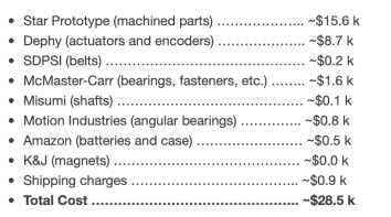
The website includes a parts lists and STEP files as well as an estimated cost ($28.5K) to build your own powered prosthetic leg. They also have a Excel spread sheet with all the parts listed, including part numbers and links to where they can be ordered (McMaster-Carr, SolidWorks, & Dephy)
They also show how to build a leg with a short youtube videoof how to assemble the whole leg as well as details for each subassembly with separate how-to videos for each.
The open source leg makes use of code from FlexSEA (Flexible Scaleable Electronics Architecture) andDephy. FlexSea was originally developed by Jean-Francois (JF) Duval while he was at MIT for his doctoral thesis. He has since joined Dephy a robotics design firm. The open source leg project uses FlexSea/Dephy code for its servo control mechanisms.
There is a GitHub Python, MatLab and C control library repo with all the code. The open source leg website also includes instructions, scripts and an image file which can be used to build your own RaspberryPi (4) controller for the leg.
The two (ankle and knee) servos are USB connected to the RPi. There are also other sensors such as the joint (servo-motor) encoders and a six axis load sensor I2C connected to the RPi. Each servo has its own 950mAh battery.
On the OSL website’s control page one can see these servos in action (with short youtube segments). They also provide instructions on how to use the open source control library to take the servo mechanisms through their paces.
Although on the OSL website’s control page I didn’t see anything which put the whole leg together to make use of it in a real world application. They did show on the Data page a youtube video with the OSL attached to a person and being used to walk up and down stairs, inclines and walking across a floor.
~~~~
Seeing as how the OSL website included STEP and PDF files for all the (machined) parts which represent $15.6K of the $28.5K, if one really wanted to do this on the cheap, one could just 3D print these parts in plastic. It would obviously not suffice mechanically for real use, but it could provide a platform for testing and developing control logic. At some point one could upgrade some or all of the plastic 3D printed parts to something more durable for use in human trials.
Another option is to purchase multiple sets of parts. The OSL website also showed price estimates for purchasing two sets of ankle and knee parts. But I’d imagine if one was so inclined, a number of researchers (hobbyists or amputees) could get together and order multiple sets of parts for reduced prices.
It’s also possible, with a lot of work, that the open source leg could be redesigned to support an open source arm-hand mechanism. This is where having 3D printed plastic parts could be extremely useful in helping to redesign the leg into an arm-hand.
SETI@home was a crowdsourced computational network that took snippets of radio spectrum, sent them to 1000s of home computers to be analyzed during idle computer time, once processed the analysis was sent back to SETI@home. It was one of the first to use a crowdsourced approach to perform data processing. The data was collected at a radio telescope, sent to SETI@home and distributed from there.
6 Factors for IOT data processing
In my post I talked about 6 factors that should help determine where data is processed. Those 6 factors included
Data size which is a measure of the amount (GB, TB or PBs) of data that is being generated at an IOT node
Data pipe availability, which is all about the networking bandwidth that’s available at the IOT node. If we are talking some sort of low-bandwidth networking access then it probably makes sense to process the data more locally and send only results of processing up the stack.
Processing criticality which indicates how important is the processing of the data. If the processing could save a life then maybe it should be done as close as possible to where the data is generated. If the data processing is less critical it could perhaps be done at other nodes in an IOT network
Processing time and infrastructure cost which is all about what sort of computational resources are required to perform the processing and how much would it cost. If processing of the data is to undergo multiple passes or requires multi-core CPUs or GPUs, moving data off the IoT node and onto a more comprehensive server to process it, could make sense.
Compliance, governance and archive requirements, which discussed the potential need for all data to be available for regulatory audits and as such may need to be available at a central location anyway so why not perform processing there.
Data information funnel, which talked about the fact that an IoT network should be configured in layers and that each layer in the stack should probably be responsible for some portion of the data processing needed by the overall system, if nothing more than compressing the information before it is sent elsewhere.
Now that I review the list, the last, Data information funnel, factor really should be a function of the other factors rather than a separate factor.
In that blog post I promised to follow it up with some examples of the logic applied to real world problems. SETI is the first one I’ve seen in the literature
SETI’s IoT processing problem
Closeup front view of one antenna of the Allan Telescope Array, a radio telescope for combined radio astronomy and SETI (Search for Extraterrestrial Intelligence) research being built by the University of California at Berkeley, outside San Francisco. The first phase, consisting of 42 6 meter dish antennas like the one shown here, was completed in 2007. Eventually it will have 350 antennas. This type of antenna is called an offset Gregorian design. The incoming radio waves are reflected by the large parabolic dish onto a secondary concave parabolic reflector in front of the dish, and then into a feed horn. A metal shroud can be seen along the bottom of the secondary reflector which shields the antenna from ground noise. It covers the frequency range from 0.5 to 11.2 GHz.
The SETI researchers found that “The telescopes are now capable of producing so much data that it’s not possible to get that volume of data out to volunteers,” And “The discovery space is in these massive, massive data streams. And it’s just not efficient to distribute many terabits per second out to volunteers all over the world. It’s more efficient for that data processing to happen at the actual observatory.”
So they moved the data processing for the SETI IoT network from being distributed out to home computers throughout the world to being done at the (telescope) source where the data was originally generated.
This decision seems to rely on a couple of the factors above. Namely the pipe availability and data size factors. They had to move processing because no pipes existed to send Tb of data to 1000s of home computers. And finally, the processing time and infrastructure cost has come down so much, that it was just easier to do the processing onsite.
It doesn’t seem like processing criticality or compliance-governance-archive had any bearing on the decision.
So there’s the first example that seems to fit well into our data processing framework.
~~~~
We ought to be able to come up with a formula that uses all these factors and comes up to with a yes or no as to whether to process the data on the node or not.
Project Natick’s Phase 2 underwater data center had 12 racks with 864 servers and 27.5PB of disk storage and was connected to the nearby Orkney island’s power grid (250Kw) and networking infrastructure. The Orkney’s islands are located off the NE coast of the Scotland and its power grid is 100% renewable, using tidal, solar and wind power. During the data center test, Orkney was able was able to power the data center, the islands and still provide power back to the Scottish power grid.
More reliable underwater
According to early reports, the servers in the underwater data center had 1/8th the failures that a control data center, on land, had. Microsoft attributes the enhanced server reliability to the use of a 100% Nitrogen (at 1 atmosphere pressure) rather than normal air and the lack of any humans to jostle the equipment/disturb the environment.
It’s also likely that the temperature variability present in a normal, on the surface of the earth, data center was measurably less than for a data center on the sea floor. If this were true, that could also help explain its better reliability.
Why underwater?
It’s all about cooling modern servers (and storage). According to NREL ( USA National Renewable Energy Lab), most data centers operate at 1.8 PUE (power use efficiency) that is, using 180% of the power required for the servers, storage and networking equipment. The other 80% is used mainly for cooling electronics, but also includes lighting, HVAC, and other essential services for humans. NREL says that high efficiency data centers can achieve a PUE of 1.2.
PUE for Project Natick Phase 2 data center was reported to be 1.07. The only additional electricity needed would probably be power for cooling.
Cooling for the Project Natick Phase 2 data center used seawater pumped through the back of server racks. The data center was placed on the seafloor at 35m (117ft) deep.
It kind looked like a submarine. According to Microsoft, the data center was contracted for, built and deployed in under 90 days. The intent was to have the data center be smaller than a standard ISO shipping container. The data center was driven ontop of an 18 wheeler, from where it was built to the Orkney Island, including ferry crossings. It was placed on a triangular support, towed out to see and deposited on the seafloor.
While 864 servers and 27.5PB of storage seem like a lot to most of us, for Microsoft Azure it’s too small to be used as a regional zone. But for (large) edge deployments. something this size or (10X) smaller might be just the thing.
Microsoft notes that 1/2 the world’s population lives within 200km (120mi) of the ocean. So there’s a ready supply of people and businesses that could take advantage of any underwater data center.
And of course, such a structure when laid on the bottom of the ocean floor, could create an artificial reef (if left in place long enough). Artificial reefs have been made out of ocean oil rigs, sunken war ships and large chunks of steel/concrete. So a underwater data center could do so just as well. And maybe the heating coming from the data center cooling pumps would foster even more coral life.
Microsoft plans Project Natick Phase 3 to be a full Azure AZ that will be deployed underwater which will include about 12 Phase 2 datacenter pressurized units.


