Tattoos that light up

Read an article the other day, titled Light-emitting tattoo engineered in ScienceDaily. Which was reporting on research done by University College London and Istituto Italiano di Tecnologia (Italian Institute of Technology) (Ultrathin, ultra-comfortable and free-standing, tattooable LEDs – behind paywall).

The new technology out of their research can construct OLEDs, found in TVs, phones, and other displays, and apply them as temporary tattoos. The tattoos will eventually degrade, wash off but while present on the skin they can light up and display information.

According to the Nanowerk news article reporting on the research, (see Light emitting tattoos engineered for the 1st time), the OLEDs are printed onto paper which can then be transferred to skin by the application of water. The picture above shows a number of the OLED tattoos ready for application.

The vision is that OLED tattoos along with other flexible electronics could provide wearable sensors of bio-chemical activity of a person. Such sensors could be used in hospitals and in the home to display dehydration, glucose status, oxygenation, etc. as well as be able to display heart and breath rates. But in order to get to that vision there’s a few steps that are needed.

Flexible, stretchable electronics

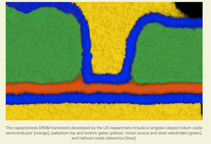
There have been a number of articles about creating flexible electronics, (e.g., see A design to improve the resilience and electrical performance thin metal film based electrodes). This article was reporting on research done at the University of Illinois, Champaign-Urbana reported in Nature (behind paywall) but one of the researchers blogged about in NaturePortfolio Devices & Materials (see: An atom-thick interlayer enables the electrical ductility of thin-film metal electrodes).

Flexible electronics can be constructed by creating a thin metal film with the electronics embedded in it placed on top of a flexible substrate. However, when that flexible substrate starts to deform or stretch it induces cracks in the thin metal films which lead to loss of conductivity, or loss of electronics function.

The research cited in the article above showed videos of cracking that takes place during deformation and stretching which would lead to loss of conductivity.

But the researchers at UofI found out that if you place a thin layer of graphene or other 2D sheet of material between the electronic thin film and the flexible substrate, the cracks that eventually happen are much less harmful to electronic conduction or functioning or provide electronic ductability. To add ductablity to an electronic circuit using LEDs the team applied an atomically thin (<1nm), 2D layer of graphene between it and the flexible substrate.

Somehow the graphene provided a mechanical buffer between the flexible substrate and the thin film electronics that allowed the circuits to have much more ductility. It appears that this mechanical buffer changed the type of cracking that occurs on the thin metal film such that they are shorter and more varied in direction rather than straight across and this helped them retain functioning longer than without the

The researchers at U of I actually created a led display that could be bent without failure. See a video of them comparing the thin film vs thin film with 2D substrate.

Skin sensors

Moreover, there have been a number of articles discussing new wearable technologies that could be used to sense a persons bio-chemical state. For example, research reported on recently (see Do Sweat It! Wearable Microfluidic Sensor to Measure Lactate Concentration in Real Time) done at the Tokyo University of Science, published in Electochimica Acta (behind paywall) talks about a sweat sensor that can be applied to skin to determine when athletes or others are getting dehydrated.

This sensor uses a micro-fluidics device which printed with electronic ink. Such a device could be manufactured in volume and be readily printed onto surfaces, that could be applied to the skin, anywhere sweat was being produced.

Future tattoos

Wearable sensors already surround us. We have watches that can tell our heart rates, walk/running speed/rates, step counts, etc. It doesn’t take much to imagine that most if not all of these could be fabricated on a thin film and with the proper 2D substrate layer be applied as a tattoo to a person while in the hospital but all these sensors have lacked a read out or display up until now. With OLED readouts wearable sensors now have a reasonable display capability.

The sweat sensor above uses microfluidics to do a lactate assay of sweat. The motion sensors in my watch uses MEMs and onboard IMU/GPS to determine speed and direction of movement. Electronic temperature sensors use thermoelectric effects. Blood oxygen sensors use LEDs and light sensors. None of these appears unable to be fabricated, miniaturized and printed on thin films. Adding OLEDs and why do we need a watch anymore?

What seems to be the most glaring omission is gas sensors (although the lactate micro-fluidic sensor is close). If we could somehow miniaturize gas sensors with enough sensitivity to glucose levels, immunological load, specific diseases (COVID19), then maybe there’d be a mass market for such devices, outside of a hospital or smart watch users.

Then with OLED and electronics that can be temporarily tattooed onto a person skin., why couldn’t this be a fashion accessory. I can imagine lot’s of people would have interest in lighting up messages, iconography or other data on their arms, hands, or other areas of a person’s body. I wonder if it could be used to display hair on the top of my head :)?

And of course these OLED-electronics based tattoos are temporary. But if they are all made from electronic ink, it seems to me that such tattoos could be permanently printed (implanted?) onto a persons skin.

Maybe at some future point a permanent OLED-electronics based tattoo could provide an electronic display and input device that could be used in conjunction with a phone or a smart-watch. All it would take would be blue-tooth.

Comments?

Photo credits:

New DRAM can be layered on top of CPU cores

At the last IEDM (IEEE International ElectronDevices Meenting), there were two sessions devoted to a new type of DRAM cell that consists or 2 transistors and no capacitors (2TOC) that can be built in layers on top of a micro processor which doesn’t disturb the microprocessor silicon. I couldn’t access (behind paywalls) the actual research but one of the research groups was from Belgium (IMEC) and the other from the US (Notre Dame and R.I.T). This was written up in a couple of teaser articles in the tech press (see IEEE Spectrum tech talk article).

DRAM today is built using 1 transistor and 1 capacitor (1T1C). And it appears that capacitors and logic used for microprocessors aren’t very compatible. As such, most DRAM lives outside the CPU (or microprocessor cores) chip and is attached over a memory bus.

New 2T0C DRAM Bit Cell: Data is written by appliying current to the WBL and WWL and bit’s are read by seeing if acurrent can pass through the RWL RBL

Memory busses have gotten faster in order to allow faster access to DRAM but this to is starting to reach fundamental physical limits and DRAM memory sizes aren’t scaling like the used to.

Wouldn’t it be nice if there were a new type of DRAM that could be easlly built closer or even layered on top of a CPU chip, with faster direct access from/to CPU cores. through inter chip electronics.

Oxide based 2T0C DRAM

DRAM was designed from the start with 1T1C so that it could hold a charge. With a charge in place it could be read out quickly and refreshed periodically without much of a problem.

The researcher found that at certain sizes (and with proper dopants) small transistors can also hold a (small) charge without needing any capacitor.

By optimizing the chemistry used to produce those transistors they were able to make 2T0C transistors hold memory values. And given the fabrication ease of these new transistors, they can easily be built on top of CPU cores, at a low enough temperature so as not to disturb the CPU core logic.

But, given these characteristics the new 2T0C DRAMB can also be built up in layers. Just like 3D NAND and unlike current DRAM technologies.

Today 3D NAND is being built at over 64 layers, with Flash NAND roadmap’s showing double or quadruple that number of layers on the horizon. Researchers presenting at IMEC were able to fabricate an 8 layer 2T0C DRAM on top of a microprocessor and provide direct, lightening fast access to it.

The other thing about the new DRAM technology is that it doesn’t need to be refreshed as often. Current DRAM must be refreshed every 64 msec. This new 2T0C technology has a much longer retention time and currently only needs to be refreshed every 400s and much longer retention times are technically feasible.

Some examples of processing needing more memory:

  • AI/ML and the memory wall -Deep learning models are getting so big that memory size is starting to become a limiting factor in AI model effectiveness. And this is just with DRAM today. Optane and other SCM can start to address some of this problem but ithe problem doesn’t go away, AI DL models are just getting more complex I recently read an article where Google trained a trillion parameter language model.
  • In memory databases – SAP HANA is just one example but they are other startups as well as traditional database providers that are starting to use huge amounts of memory to process data at lightening fast speeds. Data only seems to grow not shrink.

Yes Optane and other SCM today can solve some of thise problems. But having a 3D scaleable DRAM memory, that can be built right on chip core, with longer hold times and faster direct access can be a game changer.

It’s unclear whether we will see all DRAM move to the new 2T0C format, but if it can scale well in the Z direction has better access times, and longer retention, it’s unclear why this wouldn’t displace all current 1T1C DRAM over time. However, given the $Bs of R&D spend on new and current DRAM 1T1C fabrication technology, it’s going to be a tough and long battle.

Now if the new 2T0C DRAM could only move from 1 bit per cell to multiple bits per cell, like SLC to MLC NAND, the battle would heat up considerably.

Photo Credits:

The rise of MinIO object storage

MinIO presented at SFD21 a couple of weeks back (see videos here). They had a great session, as always with Jonathan and AB leading the charge. We’ve had a couple of GreyBeardsOnStorage podcasts with AB as well (listen and see GreyBeards talk open source S3… and GreyBeards talk Data Persistence …). We first talked with MinIO last year at SFD 19 where AB made a great impression on the bloggers (see videos here)

Their customers run the gamut from startups to F500. AB said that ~58% of the F500 have MinIO installed and over 8% of the F500 have added capacity over the last year. AB said they have a big presence in Finance, e.g., the 10 largest banks run MinIO, also the auto and Space/Defense sectors have adopted their product.

One reason for the later two sectors (auto & space/defense) is the size of MinIO’s binary, 50MB. And my guess for why the rest of those customers have adopted MinIO is because it’s S3 API compatible, it’s open source, and it’s relatively inexpensive.

Object storage trends

Customers running in the cloud have a love-hate relationship with object storage, they love that it scales but hate what it costs. There are numerous on prem object storage alternatives from traditional and non-traditional storage vendors, but most are deployed on appliances.

With appliances, customers have to order, wait for delivery, rack-configure-set up and after maybe weeks to months finally they have object storage on prem. But with MinIO a purely software, open source solution, it can be tried by merely downloading a couple of (Docker) containers and deployed/activated in under an hour..

As mentioned above, MinIO is API compatible with AWS S3 which helps with adoption. Moreover, now that it’s an integral part of VMware (see their new Data Persistence Platform), it can be enabled in seconds on your standard enterprise VMware cluster with Tanzu.

The other trend is that the edge needs storage, and lots of it. The main drivers of massive edge storage requirement are TelCos deploying 5G and auto industry’s self-driving cars. But this is just a start, industrial IoT will be generating reams of sensor log data at the edge, it will need to be stored somewhere. And what better place to store all this data, but on object storage. Furthermore, all this is driving more adoption of object storage, with MinIO picking up the lion’s share of deployments.

In addition, MinIO recently ported their software to run on ARM. AB said this was to support the expanding hobbyist and developers community driving edge innovation.

And then there was Kubernetes. Everyone in the industry (with the possible exception of Google) is surprised by the adoption of K8S. Google essentially gifted ~$1Bs in R&D on how to scale apps to the world of IT, and now any startup, anywhere, can scale with as well as Google can. And scaling is the “killer app” for the SW industry.

But performance isn’t bad either

Jonathan made mention of MinIO performance (see MinIO 24 node disk and MinIo 32 node NVMe SSD reports) benchmarks. Their disk data shows avg read and write performance of 16.3GB/s and 9.4GB/s, respectively and their NVMe SSD average read and write performance of 183.2GB/s and 171.3GB/s, respectively. The disk numbers are very good for object storage, but the SSD numbers are spectacular.

It turns out that modern, cloud native apps don’t need quick access to data as much as high data throughput. Modern apps have moved to a processing data in memory rather than off of storage, which means they move (large) chunks of data to memory and crunch on it there, and then spit it back out to storage This type of operating mode seems to scale better (in the cloud at least) than having a high priced storage system servicing a blizzard of IO requests from everywhere.

Other vendors had offered SSD object storage before but it never took off. But nowadays, with NVMe SSDs, MinIO is seeing starting to see healthcare, finance, and any AI/ML workloads all deploying NVMe SSD object storage. Yes for large storage repositories, (object storage’s traditional strongpoint), ie, 5PB to 100PB, disk can’t be beat but where blistering high throughput, is needed, NVMe SSD object storage is the way to go.

Open source vs. open core

AB mentioned that MinIO business model is 100% open source vs. many other vendors that use open source but whose business model is open core. The distinction is that open core vendors use open source as base functionality and then build proprietary, charged for, software features/functions on top of this.

But open source vendors, like MinIO offer all their functionality under an open source license (Apache SM License V2.0, GNU AGPL v3 Open Source license and other FOSS licenses), but if you want to use it commercially, build products with it embedded inside, or have enterprise class support, one purchases a commercial license.

As presented at SFD21, but their website home page has updated numbers reflected below

The pure open source model has some natural advantages:

  1. It’s a great lead gen solution because anyone, worldwide, 7X24X365 can download the software and start using it, (see Docker Hub or MinIO’s download page
  2. It’s a great hiring pool. Anyone, who has contributed to the MinIO open source is potentially a great technical hire. MinIO stats says they have 685 contributors, 19 in just the last month for MinIO base code (see MinIO’s GitHub repo).
  3. It’s a great development organization. With ~20 commits a weekover the last year, there’s a lot going on to add functionality/fix bugs. But that’s the new world of software development. Given all this activity, release frequencies increase, ~4 releases a month ((see GitHub repo insights above).
  4. It’s a great testing pool with, ~480M Docker Pulls (using a Docker container to run a standard, already configured MinIO server, mc, console, etc.) and ~18K enterprises running their solution, that’s an awful lot of users. With open source a lot of eye’s or contributors make all problems visible, but what’s more typical, from my perspective, is the more users that deploy your product, the more bugs they find.

Indeed, with the VMware’s Data Persistence Platform, Tanzu customers can use MinIO’s object storage at the click of a button (or three).

Of course, open source has downsides too. Anyone can access packages directly (from GitHub repo and elsewhere) and use your software. And of course, they can clone, fork and modify your source code, to add any functionality they want to it. Historically, open source subscription licensing models don’t generate as much revenues as appliance purchases do. And finally, open source, because it’s created by geeks, is typically difficult to deploy, configure, and use.

But can they meet the requirements of an Enterprise world

Because most open source is difficult to use, the enterprise has generally shied away from it. But that’s where there’s been a lot of changes to MinIO.

MinIO always had a “mc” (minio [admin] client) that offered a number of administrative services via an API, programmatically controlled interface. but they have recently come out with a GUI offering, the minIO console, which has a similarly functionality to their mc APU. They demoed the console on their SFD21 sessions (see videos above).

Supporting 18K enterprise users, even if only 8% are using it a lot, can be a challenge, but supporting almost a half a billion docker pulls (even if only 1/4th of these is a complete minIO deployment) can be hell on earth. The surprising thing is that MinIO’s commercial license promises customers direct-to-engineer support.

At their SFD21 sessions, AB stated they were getting ~2.7 new (tickets) problems a day. I assume these are what’s just coming in from commercial licensed users and not the general public (using their open source licensed offerings). AB said their average resolution time for these tickets was under 15 minutes.

Enter SubNet, the MinIO Subscription Network and their secret (not open source?) weapon to scale enterprise class support. Their direct-to-engineer support model involves a much, more collaborative approach to solving customer problems then you typical enterprise support with level 1, 2 & 3 support engineers. They demoed SubNet briefly at SFD21, but it could deserve a much longer discussion/demostration.

What little we saw (at SFD21) was that it looked almost like slack-PM dialog between customer and engineer but with unlimited downloads and realtime interaction.

MinIO also supports a very active Slack discussion group with ~11K users. Here anyone can ask a question and it will get answered by anyone. MinIO’s Slack has 2 channels: (Ggeneral and GitHub for notifications). It seems like MinIO is using Slack as a crowdsourced level 1 support.

But in the long run, to continue to offer “direct-to-engineer” levels of support, may require adding a whole lot more engineers. But AB seems prepared to do just that.

~~~~

MinIO is an interesting open source S3 API compatible, object storage solution that seems to run just about anywhere, is freely deployable with enterprise class support available (at a price) and has high throughput performance. What’s not to like.

cOAlition S requires open access to funded research

I read a Science article this last week (A new mandate highlights costs and benefits of making all scientific articles free) about a group of funding organizations that have come together to mandate open access to all peer-reviewed research they fund called Plan S. The list of organizations in cOAlition S is impressive including national R&D funding agencies from UK, Ireland, Norway, and a number of other countries, charitable R&D funding agencies from WHO, Welcome Trust, Bill&Melinda Gates Foundation and more, and the group is also being funded by the EU. Plan S takes effect this year.

Essentially, all research funded by these organizations must be immediately published in open access forum, open access journals or be freely available in an open access section of a publishers website which means it could be free to be read by anyone worldwide with access to the web. Authors and institutions will retain copyright for the work and the work will be published under an open access license such as the CC BY (Creative Commons Attribution) license.

Why open access is important

At this blog, frequently we find ourselves writing about research which is only available on a paid subscription or on a pay per article basis. However, sometimes, if we search long enough, we find a duplicate of the article published in pre-print form in some preprint server or open access journal.

We have written about open access journals before (see our New Science combats Coronavirus post). Much of what we do on this blog would not be possible without open access journals like PLoS, BioRxiv, and PubMed.

Open access mandates are trending

Open access mandates have been around for a while now. And even the US Gov’t got into the act, mandating all research funded by the NIH be open access by 2008, with Dept of Agriculture and Energy following later (see wikipedia Open access mandates).

In addition, given the pandemic emergency, many research publishers like Nature and Elsevier made any and all information about the Coronavirus free access on their websites.

Impacts and R&D research publishing business model

Although research is funded by public organizations such as charities and government agencies, prior to open access mandates, most research was published in peer-reviewed journal magazines which charged a fee for access. For many research organizations, those fees were a cost of doing research. If you were an independent researcher or in an institution that couldn’t afford these fees, attempting to do cutting edge research was impossible without this access.

Yes in some cases, those journal repositories waved these fees for deserving institutions and organizations but this wasn’t the case for individual researchers. Or If you were truly diligent, you could request a copy of a paper from an author and wait.

Of course, journal publishers have real expenses they needed to cover, as well as make a reasonable profit. But due to business consolidation, there were fewer independent journals around and as a result, they charged bundled license fees for vast swathes of research articles. Such a wide bundle may or may not be of interest to an individual or an institution. That plus with consolidation, profits were becoming a more significant consideration.

So open access mandates, often included funding to cover fees for publishers to supply open access. Such fees varied widely. So open access mandates also began to require fees to be published and to be supplied a description how prices were calculated. By doing so, their hope was to make such costs more transparent

Impacts on authors of research articles

Somewhere there’s an aphorism for researchers that says “publish or perish“, which means you must publish research in order to become a recognized expert in your field. Recognition often the main driver behind better academic employment and more research funding.

However, it’s not just about volume of published papers, the quality of research also matters. And the more highly regarded publishing outlets have an advantage here, in that they are de facto gatekeepers to whats published in their journals. As such, where you publish can often lend credibility to any research.

Another thing changed over the last few decades, judging the quality of research has become more quantative. Nowadays, research quality is also dependent on the number of citations it receives. The more popular a publisher is, the more readers it has which increases the possibility for citations.

Thus, most researchers try to publish their best work in highly regarded journals. And of course, these journals have a high cost to provide open access.

Successful research institutions can afford to pay these prices but those further down the totem pole cannot.

Most mandates come with additional funding to support paying the cost to supply open access. But they also require publishing and justifying these. In the belief that in doing this so it will lend some transparency to these costs.

So the researcher is caught in the middle. Funding organizations want open access to research they fund. And publishers want to be paid a profit for that access.

History of research publication

Nature magazine first started publishing research in 1859, Science magazine first published in 1880, the Royal Society first published research in 1665. So publishing research has been going on for 350 years, and at least as a for profit business model, since the mid-1800s.

Research prior to being published in journals was only available in books. And more than likely, the author of the research had to pay to have a book published and the publisher made money only when those books were sold. And prior to that, scientific research was mostly only available in a course of study, also mostly paid for by the student.

So science has always had a cost to access. What open access mandates are doing is moving this cost to something added to the funding of research.

Now if open access can only solve the reproducibility crisis in science we could have us a real scientific revolution.

Comments?

Photo Credits:

The beginning of the end of cancer

Read an article today about new research done to apply big data analytics against multiple cancer strains to identify key control mechanisms that allow cancer to survive in the body and multiply. The article Big data analysis find cancer’s key vulnerabilities discusses their discovery of 24 “master regulators” that are present in a number of different cancers. The original research article is in Cell (behind paywall) but I managed to find a preprint on BiorXiv.

From a (software) coding perspective, it’s almost like a majority of cancers are re-using the same modules to perform functions that are needed by the cancer cells. Not all cancers exhibit all master regulator blocks but all the cancers that they have examined have some of them.

The researchers examined the regulatory/signaling networks of proteins in 112 cancer cell lines. They identified 407 master regulatory proteins and further analysis showed that these protiens were associated with 24 master regulatory architectures (oncotectures). A decent laymen description of a cancer oncotecture can be found in an old (2016) Economist Article Cancer’s master criminals…

Master regulatory proteins

According to the Economist article master regulatory proteins are proteins that regulate processes in a cancer cell that cause other proteins to be made, which cause other proteins to be made, etc. which affect the way a cancer cell lives and propagates inside a body.

Biologists call these sorts of proteins transcription factors which controls the copying of DNA information into mRNA which are then taken to protein factories to create proteins from that blueprint.

The research team believe they24 master regulatory (MR) blocks, if they could be disabled somehow, would disrupt the cancer cell and ultimately eliminate that cancer from a body.

It’s almost like a DevOps script that automates the deployment of software inside the cloud. The fact that they have identified 24 master regulatory (MR blocks) architectures (sequences of proteins that are occur) that apply to a wide set of cancer tumor sub-types implies that these could be needed to regulate the functionality of these cancers. If drugs could be devised to interrupt, change or deactivate these master regulatory blocks it’s quite possible that these cancers would be eliminated.

Identifying MR Blocks using (Bio/Life Sciences) Big Data

It all starts with VIPER analysis (GitHub repo) that measures a specific proteins transcriptional activity level. In this fashion they were able to analyze the 112 tumor subtype proteome (the total complement of all proteins active in a cell). And whittle these down, using cluster analysis to those that were especially relevant for the cancer cell transcription activity.

They then used DIGGIT analysis (GitHub repo of R implementation) to identify the MR proteins and identify cellular mutations that led to them. The types of mutations can be copy number, single point or gene fusion. DIGGIT analysis can help identify which of the mutations are responsible for the protein being analyzed. The DIGGIT process is a multi-step, analytical approach to identifying candidate MR proteins.

Then using tumor checkpoint hypothesis and Bayesian analysis/integration they further ranked the MR candidate proteins. Tumor checkpoints are state transitions in the life of a cancer cell where the cell assesses its environment and then determines what actions to take next.

The tumor checkpoint hypothesis says that during the life cycle of a cancer cell it goes through various state transitions. The researchers have shown that these state transitions are managed by the MR blocks they have identified.

In the final step in their analysis, they used tumor checkpoint hypothesis and modularity with saturation & modularity analysis to identify top MR proteins and the MR blocks active in the 112 tumor subtypes.

At the end of their analysis, they had identified 24 MR blocks which solely or in some combination are present in each of the 112 tumor subtypes. If these MR blocks could be attacked by specific drugs then each of these 112 tumor subtypes could essentially be eliminated from a body or rather cure that cancer.

Photo Credit(s):

Is hardware innovation accelerating – hardware vs. software innovation (round 6)

There’s something happening to the IT industry, that maybe has not happened in a couple of decades or so but hardware innovation is back. We’ve been covering bits and pieces of it in our hardware vs software innovation series (see Open source ASiCs – HW vs. SW innovation [round 5] post).

But first please take our new poll:

Hardware innovation never really went away, Intel, AMD, Apple and others had always worked on new compute chips. DRAM and NAND also have taken giant leaps over the last two decades. These were all major hardware suppliers. But special purpose chips, non CPU compute engines, and hardware accelerators had been relegated to the dustbins of history as the CPU giants kept assimilating their functionality into the next round of CPU chips.

And then something happened. It kind of made sense for GPUs to be their own electronics as these were SIMD architectures intrinsically different than SISD, standard von Neumann X86 and ARM CPUs architectures

But for some reason it didn’t stop there. We first started seeing some inklings of new hardware innovation in the AI space with a number of special purpose DL NN accelerators coming online over the last 5 years or so (see Google TPU, SC20-Cerebras, GraphCore GC2 IPU chip, AI at the Edge Mythic and Syntiants IPU chips, and neuromorphic chips from BrainChip, Intel, IBM , others). Again, one could look at these as taking the SIMD model of GPUs into a slightly different direction. It’s probably one reason that GPUs were so useful for AI-ML-DL but further accelerations were now possible.

But it hasn’t stopped there either. In the last year or so we have seen SPUs (Nebulon Storage), DPUs (Fungible, NVIDIA Networking, others), and computational storage (NGD Systems, ScaleFlux Storage, others) all come online and become available to the enterprise. And most of these are for more normal workload environments, i.e., not AI-ML-DL workloads,

I thought at first these were just FPGAs implementing different logic but now I understand that many of these include ASICs as well. Most of these incorporate a standard von Neumann CPU (mostly ARM) along with special purpose hardware to speed up certain types of processing (such as low latency data transfer, encryption, compression, etc.).

What happened?

It’s pretty easy to understand why non-von Neumann computing architectures should come about. Witness all those new AI-ML-DL chips that have become available. And why these would be implemented outside the normal X86-ARM CPU environment.

But SPU, DPUs and computational storage, all have typical von Neumann CPUs (mostly ARM) as well as other special purpose logic on them.

Why?

I believe there are a few reasons, but the main two are that Moore’s law (every 2 years halving the size of transistors, effectively doubling transistor counts in same area) is slowing down and Dennard scaling (as you reduce the size of transistors their power consumption goes down and speed goes up) has stopped almost. Both of these have caused major CPU chip manufacturers to focus on adding cores to boost performance rather than just adding more transistors to the same core to increase functionality.

This hasn’t stopped adding instruction functionality to each CPU, but it has slowed considerably. And single (core) processor speeds (GHz) have reached a plateau.

But what it has stopped is having the real estate available on a CPU chip to absorb lots of additional hardware functionality. Which had been the case since the 1980’s.

I was talking with a friend who used to work on math co-processors, like the 8087, 80287, & 80387 that performed floating point arithmetic. But after the 486, floating point logic was completely integrated into the CPU chip itself, killing off the co-processors business.

Hardware design is getting easier & chip fabrication is becoming a commodity

We wrote a post a couple of weeks back talking about an open foundry (see HW vs. SW innovation round 5 noted above)that would take a hardware design and manufacture the ASICs for you for free (or at little cost). This says that the tool chain to perform chip design is becoming more standardized and much less complex. Does this mean that it takes less than 18 months to create an ASIC. I don’t know but it seems so.

But the real interesting aspect of this is that world class foundries are now available outside the major CPU developers. And these foundries, for a fair but high price, would be glad to fabricate a 1000 or million chips for you.

Yes your basic state of the art fab probably costs $12B plus these days. But all that has meant is that A) they will take any chip design and manufacture it, B) they need to keep the factory volume up by manufacturing chips in order to amortize the FAB’s high price and C) they have to keep their technology competitive or chip manufacturing will go elsewhere.

So chip fabrication is not quite a commodity. But there’s enough state of the art FABs in existence to make it seem so.

But it’s also physics

The extremely low latencies that are available with NVMe storage and, higher speed networking (100GbE & above) are demanding a lot more processing power to keep up with. And just the physics of how long it takes to transfer data across a distance (aka racks) is starting to consume too much overhead and impacting other work that could be done.

When we start measuring IO latencies in under 50 microseconds, there’s just not a lot of CPU instructions and task switching that can go on anymore. Yes, you could devote a whole core or two to this process and keep up with it. But wouldn’t the data center be better served keeping that core busy with normal work and offloading that low-latency, realtime (like) work to a hardware accelerator that could be executing on the network rather than behind a NIC.

So real time processing has become faster, or rather the amount of time to execute CPU instructions to switch tasks and to process data that needs to be done in realtime to keep up with faster line speed is becoming shorter.

So that explains DPUs, smart NICS, DPUs, & SPUs. What about the other hardware accelerator cards.

  • AI-ML-DL is becoming such an important and data AND compute intensive workload that just like GPUs before them, TPUs & IPUs are becoming a necessary evil if we want to service those workloads effectively and expeditiously.
  • Computational storage is becoming more wide spread because although data compression can be easily done at the CPU, it can be done faster (less data needs to be transferred back and forth) at the smart Drive.

My guess we haven’t seen the end of this at all. When you open up the possibility of having a long term business model, focused on hardware accelerators there would seem to be a lot of stuff that needs to be done and could be done faster and more effectively outside the core CPU.

There was a point over the last decade where software was destined to “eat the world”. I get a lot of flack for saying that was BS and that hardware innovation is really eating the world. Now that hardtware innovation’s back, it seems to be a little of both.

Comments?

Photo Credits:

Open source digital assistant

I’ve come by and purchased a number of digital assistants over the last couple of years from both Google and Amazon but not Apple. At first their novelty drove me to take advantage of them to do a number of things. But over time I started to only use them for music playing or jokes. But then I started to hear about some other concerns with the technology.

The problems with today’s vendor based, digital assistants

My and others main concern was their ability to listen into conversations in the home and workplace without being queried. Yes, there are controls on some of them to turn off the mic and thus any recordings. But these are not hardwired switches and as software may or may not work depending on the implementation. As such, there is no guarantee that they won’t still be recording audio feeds even with their mic (supposedly) turned off.

At one point I saw a news article where police had subpoenaed recordings of a digital assistant to use in a criminal case. Now I’m ok with use of this for specific, court approved, criminal cases but what’s to limit its use to such. And not all courts, or governments for that matter, are as protective of personal privacy as some.

Open source digital assistant on the way

But with an open source version of a digital assistant, one where the user had complete programmatical control over its recording and use of audio data is another matter. I suppose this doesn’t necessarily help the technically challenged among us that can’t program our way out of a paper bag but even for those individuals, the fact that an open source version exists to protect privacy, could be construed as something much more secure than a company or vendor’s product.

All that made it very interesting when I saw an article recently about a project put together at Standford on an Open source challenger to popular virtual assistants”.

How to create a open source digital assistant

The main problem facing an open source digital assistant is the need for massive amounts of annotated training request data. This is one of the main reasons that commercial digital assistants often record conversations when not specifically requested.

But Stanford University who is responsible for creating the open source digital assistant above has managed to design and create a “rules based” system to help generate all the training data needed for a virtual assistant.

With all this automatically generated training data they can use it to train a digital assistant’s natural language processing neural network to understand what’s being asked and drive whatever action is being requested.

At the moment the digital assistant (and its conversation generator) has somewhat limited skills, or rather only works in a restricted set of domains such as restaurants, people, movies, books and music. For example, “identify a restaurant near me that has deep dish pizza and is rated greater than 4 on a 5 point scale”, “find me an mystery novel talking that is about magic”, or “who was the 22nd president of the USA”.

But as the digital assistant and its annotated, rules based conversation generator are both open source, anyone can contribute more skills code or add more conversational capabilities. Over time, if there’s enough participation, perhaps even someday perform all of the skills or capabilities of commercial digital assistants.

Introducing Almond and Stanford’s OVAL

Stanford work on this project is out of their OVAL (Open Virtual Assistant Lab). Their open source virtual assistant is called Almond.

Almond’s verbal generator is called Genie and uses compositional technology to generate conversations that are used to train their linguistic user interface (LUInet). Almond also uses ThingTalk a new declaritive program language to process responses to queries and requests. Finally, Almond makes use of Thingpedia, a repository of information about internet services and IoT devices to tell it how to interact with these systems.

Stanford Genie technology

The technology behind Genie is based on using source text statements to create templates that can generate sentences for any domain you wish to have Almond work in. If one is interested in expanding the Almond domains, they can create their own templates using the Genie toolkit.

One essentially provides a small set of input sentences that are converted into templates and used by Genie to understand how to parse all similar sentences. This enables Almond to “understand” what’s being requested of it

The set of input sentences can start small and be augmented or added to over time to handle more diverse or complex queries or requests. Their GitHub toolkit and Genie technology is described more fully in a paper Genie: A generator of natural language symantec parsers for virtual assistant commands

Stanford ThingTalk declarative language

ThingTalk is the programming language used to control what Almond can do for requests and queries. Essentially it’s a multi-part statement about what to do when a request comes along. The main parts in a ThingTalk statement include:

  1. When a particular action is supposed to be triggered.
  2. What service does the request need in order to perform its action.
  3. What action is requested

The “what service does a request need” are based on Open API calls (See ThingPedia below). The “what action is requested” can either be standard Almond actions or invoke other ThingPedia open source API calls, such as create a tweet, post on FB, send email etc.

For example, a ThingTalk statement looks like:

monitor @com.foxnews.get() => @com.slack.send();

Which monitors Fox news for any new news articles and sends them (the link) to your Slack channel.

Stanford Thingpedia

Thingpedia is an open source repository of structured information available on the Web and of API services available on the web. Structured information or data is the information behind calendars, contact databases, article repositories, etc. Any of which can be queried for information and some of which can be updated or have actions performed on them. API services are the way that those queries and actions are performed.

One page of the Thingpedia multi-page summary of services that are offered

The Thingpedia web page shows a number of services that already have Open source APIs defined and registered. For example, things like twitter, facebook, bing search, BBC news, gmail and a host of other services. More are being added all the time and these represent the domains that Almond can be used to act upon.

Some of these domains are more defined that others. But in any case any service that takes the form of an web based API can be added to Thingpedia.

Thingpedia as a standalone open source repository is valuable in and of itself regardless of its use by Almond. But Almond would be impossible without Thingpedia. Thingpedia wants to be the wikipedia of APIs.

Almond, putting it all together

Almond consists of mainly the Almond Agent, Engine and Thingpedia. The Agent is used by the various Almond implementions to parse and understand the request and access the ThinkTalk program statement. Almond Agent uses its LUInet natural language interpreter, interpret that request and to select the ThingTalk program for the request. Once the ThinkTalk program is identified, it uses the various Thingpedia APIs requested by the ThinkTalk statement to generate the proper API calls to the service being requested and generate any output that is requested.

Where can you run Almond

Almond is available currently as a web app, an Android App, a Gnome (Linux) desktop/laptop App, a CLI application or can be run on your Mac or Windows computers. You could of course create your own smart speaker to run Almond or perhaps hack a current smart speaker to do so.

One important consideration is that with the Android app, all your data and credentials are only stored on the phone. And will not go out into the cloud or elsewhere. I didn’t see similar statements about privacy protections for the web app or any of the other deployments. But as Almond is open source, you potentially have much greater control over where your data resides.

~~~~

What I would really like is a smart speaker app running on a RPi with a microphones and a decent speaker attached, all in the package of a cube or cylinder.

I thought their videos on Almond were pretty cheesy but the technology is very interesting and could potentially make for an interesting competitor of today’s smar

Photo Credit(s):

All photos and graphics from Stanford Almond and OVAL Lab websites.

An Open Source Powered Leg

I read an article a couple of weeks back about an Open Source Bionic Leg, which was reporting on research began as a NSF funded project at the University of Michigan (UoM), with collaboration from Northwestern, University of Texas at Dallas and CMU. UofM has a website that provides everything you need to build your own open source leg (OSL) leg at OpenSourceLeg.com.

The challenge in human prosthetics these days is that all research is done in silos. Much of it is proprietary and only available within corporations but even university research has been hampered by the lack of a standard platform that could be used to develop new components and ideas on.

The real difficulty is defining the control logic (code). The OSL project is intended to resolve this lack of a platform by providing everything a researcher (hobbyist, or amputee) needs to build their own, at home or in the lab.

The website includes a parts lists and STEP files as well as an estimated cost ($28.5K) to build your own powered prosthetic leg. They also have a Excel spread sheet with all the parts listed, including part numbers and links to where they can be ordered (McMaster-Carr, SolidWorks, & Dephy)

They also show how to build a leg with a short youtube video of how to assemble the whole leg as well as details for each subassembly with separate how-to videos for each.

The open source leg makes use of code from FlexSEA (Flexible Scaleable Electronics Architecture) and Dephy. FlexSea was originally developed by Jean-Francois (JF) Duval while he was at MIT for his doctoral thesis. He has since joined Dephy a robotics design firm. The open source leg project uses FlexSea/Dephy code for its servo control mechanisms.

There is a GitHub Python, MatLab and C control library repo with all the code. The open source leg website also includes instructions, scripts and an image file which can be used to build your own RaspberryPi (4) controller for the leg.

The two (ankle and knee) servos are USB connected to the RPi. There are also other sensors such as the joint (servo-motor) encoders and a six axis load sensor I2C connected to the RPi. Each servo has its own 950mAh battery.

On the OSL website’s control page one can see these servos in action (with short youtube segments). They also provide instructions on how to use the open source control library to take the servo mechanisms through their paces.

Although on the OSL website’s control page I didn’t see anything which put the whole leg together to make use of it in a real world application. They did show on the Data page a youtube video with the OSL attached to a person and being used to walk up and down stairs, inclines and walking across a floor.

~~~~

Seeing as how the OSL website included STEP and PDF files for all the (machined) parts which represent $15.6K of the $28.5K, if one really wanted to do this on the cheap, one could just 3D print these parts in plastic. It would obviously not suffice mechanically for real use, but it could provide a platform for testing and developing control logic. At some point one could upgrade some or all of the plastic 3D printed parts to something more durable for use in human trials.

Another option is to purchase multiple sets of parts. The OSL website also showed price estimates for purchasing two sets of ankle and knee parts. But I’d imagine if one was so inclined, a number of researchers (hobbyists or amputees) could get together and order multiple sets of parts for reduced prices.

It’s also possible, with a lot of work, that the open source leg could be redesigned to support an open source arm-hand mechanism. This is where having 3D printed plastic parts could be extremely useful in helping to redesign the leg into an arm-hand.

Photo Credit(s):